nickagian
Member level 4
- Joined
- Mar 19, 2009
- Messages
- 71
- Helped
- 2
- Reputation
- 4
- Reaction score
- 2
- Trophy points
- 1,288
- Location
- Zurich, Switzerland
- Activity points
- 2,001
Hi,
In a system of ours, we have a CPU that is connected over PCIe with an on-board FPGA.
CPU is root complex, compliant with 2.0 and 1.0 and the FPGA is the endpoint (only 1.0 compliant).
Unfortunately the CPU tells me that the link is down (it's a new design, I have never seen it come up yet).
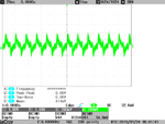
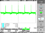
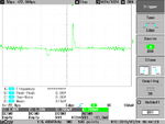
Attached you can see what I measure at the two data lines.
The 100MHz is there and running. It is created from the CPU and sent directly to the FPGA.
It seems to me as if the RC sends some kind of beacon to detect possible EP. But the question is why my EP doesn't respond or why the RC doesn't recognize the response.
Is there anyone with experience on PCIe that could help me debug? I am almost without any ideas on how to proceed.
I have thought the following:
- That the Quality of the clock is not good enough and that's why the FPGA doesn't respond, but the truth is I cannot check this with much detail.
- Wrong signal levels. If I am not mistaken, this is not the case.
- The schematics are correct. I have the necessary AC blocking capacitors on all lines, TX are connected with RX.
- The length of the Signal lines is not more than 25cm (Maximum recommended is around 50cm)
Nikos
In a system of ours, we have a CPU that is connected over PCIe with an on-board FPGA.
CPU is root complex, compliant with 2.0 and 1.0 and the FPGA is the endpoint (only 1.0 compliant).
Unfortunately the CPU tells me that the link is down (it's a new design, I have never seen it come up yet).
Attached you can see what I measure at the two data lines.
The 100MHz is there and running. It is created from the CPU and sent directly to the FPGA.
It seems to me as if the RC sends some kind of beacon to detect possible EP. But the question is why my EP doesn't respond or why the RC doesn't recognize the response.
Is there anyone with experience on PCIe that could help me debug? I am almost without any ideas on how to proceed.
I have thought the following:
- That the Quality of the clock is not good enough and that's why the FPGA doesn't respond, but the truth is I cannot check this with much detail.
- Wrong signal levels. If I am not mistaken, this is not the case.
- The schematics are correct. I have the necessary AC blocking capacitors on all lines, TX are connected with RX.
- The length of the Signal lines is not more than 25cm (Maximum recommended is around 50cm)
Nikos