needforspeed
Member level 1
Hi guys,
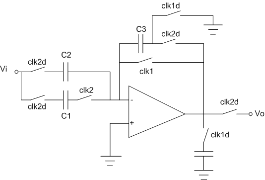
A PD(proportional plus derivative) cell was designed and fabricated, as shown in the following figure.
Ideally, we have Vo[n]=-((C1+C2)/C3)Vi[n]+(C1/C3)Vi[n-1], which is what we get in simulation. However, measurement result is Vo[n]=-((C1+C2)/C3)Vi[n]+(C1/C3)Vi[n-1]+Con. Con is a constant, about -250mV. This DC offset is not acceptable in our system.
I have no idea why this DC offset happen after fabrication, and how to minimize it. Do you have any idea about it? Thanks in advance.