gag2000
Member level 5
Dear all,
I have to design a DAC.
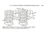
To understand different architectures, I draw an ideal 2bit subdac in order to build 1V 4 bit DAC, and tried to made the schematic 10.3-6 of "CMOS Analog Circuit Design" from Allen and Hollberg work.
I used ideal opamp with a 1V reference on the positive input.
There is something I do not understand : after the first opamp (A1 on the picture) the output has the opposite polarity of the second opamp (A2) : how can the charges be added with this schematic ?
A Spectre simulation gives me something very strange, with a positive input at the output of A1 (yellow) but the charge are added (or substracted, anyway not in the right direction) to the second stage, which gives the green output.
May you help me to understand how this circuit works !
Regards,
RG

