Continue to Site

Welcome to EDAboard.com

Welcome to our site! EDAboard.com is an international Electronics Discussion Forum focused on EDA software, circuits, schematics, books, theory, papers, asic, pld, 8051, DSP, Network, RF, Analog Design, PCB, Service Manuals... and a whole lot more! To participate you need to register. Registration is free. Click here to register now.

Custom polygon's connection style

MISU.RSG

Member level 1
Joined
Apr 29, 2011
Messages
34
Helped
2
Reputation
4
Reaction score
2
Trophy points
1,288
Activity points
1,581
Hi

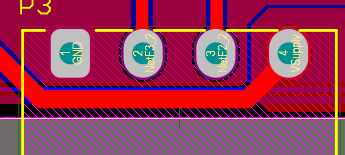
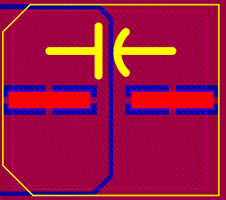
I use Altium Designer. I need to have several connection types in the same polygon. some component direct connection and some components relief connection.
how can I do it?
1705484488808.png

1705484536482.png
 
I do not use thermal relief on outer layers on SMD pads, never. Many SMPS SMD designs require a good connection both for current requirements and thermal requirements (getting heat away from the components). PTH components will be decided by the amount of copper connected and on how many layers the PTH pin connects to the copper.
I do not know the exact method of choosing whether thermal relief is used on a pad or not in Altium...
 

LaTeX Commands Quick-Menu:

Part and Inventory Search

Welcome to EDABoard.com

Sponsor

Back
Top