Continue to Site

Welcome to EDAboard.com

Welcome to our site! EDAboard.com is an international Electronics Discussion Forum focused on EDA software, circuits, schematics, books, theory, papers, asic, pld, 8051, DSP, Network, RF, Analog Design, PCB, Service Manuals... and a whole lot more! To participate you need to register. Registration is free. Click here to register now.

Current sense transformers on ETD type bobbins?

Status
Not open for further replies.
thanks, there are loads out there, but above 27Amps and there are few in stock on digikey or farnell. I reckon there will be constant supply issues.
Actually, Many Thanks to Sunnyskyguy who solved this thread inadvertently a few weeks back...Sunnyskyguy pointed out that ETD/efd etc cores, if not expensively lapped, have dramatically reduced permeability. (Also, if the cores are not properly mated with a custom jig, then the same again).
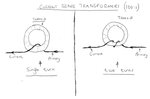
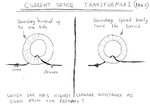
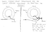
This potential massive reduction in etd core permeability, can mean far more secondary magnetising current than wanted, meaning signal distortion........I see now that unless expensive jigs and lapped cores are available, torroids are the only way to go for CSTs.

Thread #8 of this shows Sunnyskyguys great solution to this problem.....torroids are the way forward..
https://www.edaboard.com/threads/341980/
 
Last edited by a moderator:

According to my experience, loss of permeability with E- and similar core shapes is more a problem of inappropriate processing. But toroid cores have some advantages, they are e.g. best suited to realize large isolation voltage.

If you plan instrument production beyond prototype quantities, there's always the option to get the devices custom made with a clear specification.
 

thanks, by "inappropriate processing" you mean the person forgot to specify that core halves should be lapped?
 

No, I meaned using unsuitable glue or not pressing the core halves correctly. The ungapped cores have an AL specification which can be achieved with correct processing.
 

Could you please advise that in the attached diagram, the Left hand diagram is a one turn CST, and the left hand diagram is a two-turn CST?

- - - Updated - - -

I appreciate Kirchoffs law says the LHS one is a single turn, but I believe there must be some parameter detriment from the potential wide area encircled by the one turn one on the left, also out of the two toroids with bunched/evenly spaced windings, do you know which has the biggest leakage inductance as seen from the primary?
 

Attachments

  • Current sense transformers.jpg
    Current sense transformers.jpg
    47.3 KB · Views: 67
  • Leakage in CST's.jpg
    Leakage in CST's.jpg
    79.9 KB · Views: 74
Last edited by a moderator:

which has the biggest leakage inductance as seen from the primary?

I'm not totally sure to state this, but I presume that the fact to do not twist the wire right after the winding, this would produce a most significant leakage inductance if compared to other effects nearby the core.
 

thanks, so I believe you are implying that to reduce leakage, the secondary must be evenly spread right round the whole torroid circumference?
 

I was just attempting to underline that regardless the wiring dispersion schema you decide on the primary/secondary, it seems that the "half-turn" effect of the primary winding would produce a leakage inductance much more significant than any other factor related to the wire scattering geometry.

Are you willing to twist both sides like that ?

IMG_0694.JPG
 

..or must the 100 secondaries be clumped into one little bit of the torroid circumference, the same bit that the primary goes near? (in order to reduce leakage inductance)
This is for a 45khz boost pfc.

- - - Updated - - -

Are you willing to twist both sides like that ?
thanks, I will try, but the primary carries 20 Amps of current, so it wont be easy to twist, but it seems a good idea.
 

Twisting with only 1 spin should suffice to ensure a minimal leakage magnetic field flowing outside toroid path due to this action would close a loop embracing the ferrite exclusively, furthermore it would also reduce current induction reaching the PCB tracks right below the core.
 

I presume that the fact to do not twist the wire right after the winding, this would produce a most significant leakage inductance if compared to other effects nearby the core.
The loop spanned by the primary conductor definitely matters. Lack of the return path creates a partly unspecified geometry in your drawing.

so I believe you are implying that to reduce leakage, the secondary must be evenly spread right round the whole torroid circumference?
andre_luis wasn't talking about this point at all. In my view, the left uneven winding geometry gives a slightly higher leakage inductance. The right evenly spaced winding is better but not necessarily optimal. As previously mentioned, a single turn is asymmetrical by nature (unless you have a coaxial return). As a result, you'll get the lowest leakage with the secondary winding concentrated under the primary loop.

- - - Updated - - -

The transformer shown in post #28 involves additional leakage due to the separated windings.
 

The loop spanned by the primary conductor definitely matters. Lack of the return path creates a partly unspecified geometry in your drawing.
the loop of the primary is the mosfet loop of the boost pfc stage.....the CST is in the drain connection of the boost pfc fet, so the loop of the primary is through the input capacitor (1uF) , then through the boost inductor, then through the CST primary, then through the fet, then back to the input capacitor. Is this going to mean loads of leakage unless I put in the twist as shown by Andre Luis?
 

the CT with the least primary energy stored in the transformer will have the lowest leakage. But a certain minimum inductance is required based on f, current, voltage, high K value of core and geometry of core to transfer the energy to the secondary winding for a current ratio of 100:1 typical.

Too high a values may cause core eddy current losses, but you want to have some margin for surge currents to prevent saturation, so over design it to prevent remenance.
 

Is this going to mean loads of leakage unless I put in the twist

I would be more concerned to the uncertainty on the effective ratio turns seen by secondary. Assuming at assemblage manufacturing process certain dispersion on the spatial wire shapes, as well at its physical mounting on the circuit board, in theory would be expected petty different "antenna" characteristics and sensibilities.

An additional issue is that the high rate on windings ( 1:100 ) produce a high gain transformer, and the smaller difference noticed at parts of the same lot would be multiplied by a big factor, what mean that would become imperative to do a further adjustment on output resistor in order to the current transformer as a whole meet the average performance specified.
 

Would you agree that it is too risky to get SMPS current sense transformers wound onto ETD type bobbins? After all, if the winders forget to actually cross the primary wire back over itself then the primary may have zero coupling with the secondary, as the attached shows.
As you know, this can't happen with toroid cores since the winding is taken through the centre of the toroid, and therefore, there is always a completed turn of primary coupling up with the secondary.
So do you agree that its best not to wind current sense transformers on ETD type bobbins?

In the attachement, the winder has wound the primary round the bobbin in both cases, but in one picture, it doesn't end up forming a whole turn round the bobbin, which is bad.


For a mature transformer factory, they shoud have mature manufacture technology, e.g. test turns and inductance value and Q value, they can find the faliure part by these testing proceses, so no problem, thanks!
 

the loop of the primary is the mosfet loop of the boost pfc stage.....the CST is in the drain connection of the boost pfc fet, so the loop of the primary is through the input capacitor (1uF) , then through the boost inductor, then through the CST primary, then through the fet, then back to the input capacitor. Is this going to mean loads of leakage unless I put in the twist as shown by Andre Luis?
Basically yes. Presumedly you can't "twist" the primary circuit completely, but reducing the area spanned between forward and return current path is essential for a low inductance design. Implementing the wiring as superimposed PCB planes, or even as a sandwich of multiple interleaved planes are examples how at least part of the circuit can be made with very low inductance.
 

Thanks, we will naturally make the mosfet power switch loop as narrow in area as possible, so as to minimise its stray inductance. Though, having done that, can we reduce the CST leakage inductance, as seen from the primary, by twisting the primary wires as they go into the CST, as Andre Luis suggested?

As such, in the attached diagram, which Current sense transformer (CST) has the most leakage inductance, as seen from the primary? We need to minimise this leakage inductance, because the CST is situated in the Power FET loop of a boost converter PFC stage driven by UCC28070 driver. (as seen on page 1 off ucc28070 datasheet)

UCC28070 datasheet
https://www.ti.com/lit/ds/symlink/ucc28070.pdf

For a mature transformer factory, they shoud have mature manufacture technology, e.g. test turns and inductance value and Q value, they can find the faliure part by these testing proceses, so no problem
..at first we just need a few prototypes, and no manufacturer will do such low volume for us, we have to do it ourselves, there is nothing "in stock" off the shelf at this high current level (39 Amps peak, 26 Amps average)
 

Attachments

  • Leakage inductance with twisted primary CST.jpg
    Leakage inductance with twisted primary CST.jpg
    70.5 KB · Views: 83

As such, in the attached diagram, which Current sense transformer (CST) has the most leakage inductance, as seen from the primary?

Once the inductance is calculated taking into account the number of turns multiplied by the free area inside the wires, the first picture would produce a higher stray inductance along the wire pair. Note that twisting the wires with as much spins as you can, it will also make it a few less susceptible to induced current from electromagnetic fields around the core, due each loop tends to cancel the effect sensed by the neighbor loop, therefore increasing the differential-mode noise immunity.
 
  • Like
Reactions: treez

    T

    Points: 2
    Helpful Answer Positive Rating
the first picture would produce a higher stray inductance along the wire pair
-thanks, I agree that the stray wiring inductance of the picture on the Left hand side is greater than in the right hand side one. However, which one has the most transformer leakage inductance, as seen from the primary?

Also, which of the following two CST's has more leakage inductance, as seen from the primary?...the one with the primary and secondary bunched together, or the one where the secondary is spread evenly around the torroid core?

Current sense transformer winding arrangement & leakage inductance.jpg
 

which Current sense transformer (CST) has the most leakage inductance, as seen from the primary?
Still incomplete drawings. Where's the return path?

I don't see what's the point of distinguishing transformer leakage and wiring inductance. Electrically they are indistinguishable.
 
  • Like
Reactions: treez

    T

    Points: 2
    Helpful Answer Positive Rating
Status
Not open for further replies.

Similar threads

Part and Inventory Search

Welcome to EDABoard.com

Sponsor

Back
Top