Continue to Site

Welcome to EDAboard.com

Welcome to our site! EDAboard.com is an international Electronics Discussion Forum focused on EDA software, circuits, schematics, books, theory, papers, asic, pld, 8051, DSP, Network, RF, Analog Design, PCB, Service Manuals... and a whole lot more! To participate you need to register. Registration is free. Click here to register now.

Current limiter using MCU

Status
Not open for further replies.

gauravkothari23

Advanced Member level 2
Joined
Mar 21, 2015
Messages
640
Helped
5
Reputation
10
Reaction score
4
Trophy points
1,298
Activity points
6,922
Hi all.
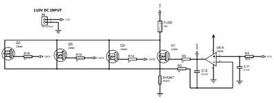
I have a project where i have to drop the current from 0.7A to 5A as per the user selection. (Circuit Attached).
As per the circuit. i have interfaced 3 buttons, SET, UP and DOWN for the user to select the amount of current to be grounded.
Am using 220V to 12V SMPS and 7805 Regulator to power the MCU (Not show in circuit diagram)
110V DC INPUT is an external input from where the voltage input would be 110V DC and 25 to 50 Amps of Current.
what my purpose is as soon as the i receive 110V DC input, 0.7A to 5A as per the user selection has to be straight away grounded, for which i am using Mosfet Q1. and shunt resistor. and rest of the current will be sent to 110V DC LOAD OUTPUT.

I am using U3(PC817) to detect 110V DC Input.
I Will control the current to be grounded using PWM and will monitor the current using shunt resistor using ADC pin of MCU.
What my problem is, when the mosfet gets ON during PWM, huge amount of current will flow through the mosfet which will OFF the 110V DC LOAD OUTPUT for a specific period of time.
Can any body please recommened me any idea for how can i do this. or what kind of circuit has to be implemented.

Current Limiter.png
 

Hi,

my opinion:
* the optocoupler is useless. Two resistors will do. (indeed I don´t see the need for detecting 110V at all)
* PWM in the meaning of "switching" makes no sense here
* Q1 to be HIGH side makes no sense here

-->
* use an LPF to generate DC from PWM
* use a N-CH MOSFET
* use an OPAMP as constant current regulator (input DC_from_PWM, output MOSFET_gate, feedback via shunt)

Classic style used million times... million documents in the internet

Klaus
Is this something what you recommend using an Op amp.
But how can i control it using an microcontroller and vary the current to be grounded as per the user input Selection.

--- Updated ---


Ok, i got it
i need to genetate PWM from Controller and then i have to use LPF filter to convert DC from PWM which would be used as a input pin of Op amp.
am i right..??

Op AMp.png
 
Last edited:

Hi,

basically yes.
It should work this way.

Some details:

* you need to divide down the PWM_DC signal to match your shunt voltage
* you should add a fast acting fuse
* I recommend to add local feedback to the OPAMP to improve stability:
--> add a 1k from shunt to inverting OPAMP input
--> add a 1nF capacitor from OPAMP_output to inverting input
--> use a "unity gain stable" OPAMP

Mind: the MOSFET will generate 550W of heat. This is a lot. It may be enough to heat your room.
It will need proper heatsinking with fan.

Klaus
 

The power consumed by the programmable load can be either dissipated in the power transistor, if it's operated in linear mode or must be transfered to a sink circuit, e.g. a load resistor. The circuit in post #1 doesn't implement any functional concept, in addition it uses a P-channel MOSFET which can't even switch in the shown configuration.

Designing an electronic load should start with some basic considerations like "how to dissipate the consumed power".
 

You have to be concerned with OpAmp stability due to MOSFET gate C load
on its output.

Here is a basic design that handles the HV drive, adds a zero to control loop to lift
phase margin (I think), and decouples the C load from OpAmp output.

Of course you can change the circuit to meet needs.

1664972784103.png


Question, do you want grounded load, source driving current to ground, or
high side pulling current from Vsupply thru load ?

Note above design for mA, can easily be scaled. Mirror can be done with
bipolars or MOSFETs, bipolars probably easiest mirror needs matching
between transistors in mirror.

A pulse input is show in diagram as author was evaluating transient response.


Regards, Dana.
 
Last edited:
Hi,

basically yes.
It should work this way.

Some details:

* you need to divide down the PWM_DC signal to match your shunt voltage
* you should add a fast acting fuse
* I recommend to add local feedback to the OPAMP to improve stability:
--> add a 1k from shunt to inverting OPAMP input
--> add a 1nF capacitor from OPAMP_output to inverting input
--> use a "unity gain stable" OPAMP

Mind: the MOSFET will generate 550W of heat. This is a lot. It may be enough to heat your room.
It will need proper heatsinking with fan.

Klaus
Agreed.
How should I connect N channel mosfet. Do I need to add any dummy load on drain pin or can connect mosfet drain pin to 110V DC and source pin to GND using shunt resistor.
 

Hi,

basically doing the connections according schematic is the way to go.

You need to be sure to stay within the specifications given in the MOSET datasheet.
If you expect some transients (like ESD) then add protection devices.

We don´t know what power supply voltage you want to use .. also OPAMP, MOSFET....

Also we don´t know the technical requirements of your application about accuracy, noise, reaction time....

Thus it´s hard to give detailed assitence.

Klaus
 

Hi,

basically yes.
It should work this way.

Some details:

* you need to divide down the PWM_DC signal to match your shunt voltage
* you should add a fast acting fuse
* I recommend to add local feedback to the OPAMP to improve stability:
--> add a 1k from shunt to inverting OPAMP input
--> add a 1nF capacitor from OPAMP_output to inverting input
--> use a "unity gain stable" OPAMP

Mind: the MOSFET will generate 550W of heat. This is a lot. It may be enough to heat your room.
It will need proper heatsinking with fan.

Klaus
Yes, Thanks.
To avoid load on single mosfet, i would be using 4 to 5 mosfets in parallel to distribute the load.
But how should i connect


The above might help.


Regards, Dana.
 
Hi,

basically doing the connections according schematic is the way to go.

You need to be sure to stay within the specifications given in the MOSET datasheet.
If you expect some transients (like ESD) then add protection devices.

We don´t know what power supply voltage you want to use .. also OPAMP, MOSFET....

Also we don´t know the technical requirements of your application about accuracy, noise, reaction time....

Thus it´s hard to give detailed assitence.

Klaus
Thanks,
I have attached the revised circuit and have designed using OP AMP LM358. i would be controlling the current through mosfet 20N60 which are 4 in parallel using PWM which is being supplied to pin 3 (Non Inverting Input) of LM358 using LPF.
But i have a problem,
When the system is powered ON, the controller will take at-least 1 to 2 mSec to get ON and to configure the port PIN 0.5 as PWM. by the time the PIN 3 of LM358 will be charged by 5V, which would make the mosfet ON for that specific period of time, where a huge amount of current would be passed through mosfet to GND. which has not to be done. how can i avoid this.
 

Attachments

  • Op AMP Driver.png
    Op AMP Driver.png
    52.6 KB · Views: 174

A weak pull-down resistor at GPIO output should be sufficient to avoid unwanted turn on during reset state.
The circuit has however a problem. Gate threshold voltage variations will cause unequal curren sharing between MOSFETs. Need to increase the shunt resistance considerably.
 

A weak pull-down resistor at GPIO output should be sufficient to avoid unwanted turn on during reset state.
The circuit has however a problem. Gate threshold voltage variations will cause unequal curren sharing between MOSFETs. Need to increase the shunt resistance considerably.
Sure will add Weak Pull up Resistor.
For gate threshold voltage, can i add, a transistor BC547.
Base to Op amp output with 1K current limiting resistor.
Collector with 1K resistor to 12V and mosfet Gate Pin.
Emitter to GND.

So in this case, even my Unwanted turn ON of Mosfet at reset will also be solved.
 

Other than told in post #12, the problem of unequal current sharing can be only solved with individual source series resistors or separate measurement shunts and control amplifiers.
 

Other than told in post #12, the problem of unequal current sharing can be only solved with individual source series resistors or separate measurement shunts and control amplifiers.
sorry, bit confused.
do you mean i have to add 4 shunt resistors to individual mosfet with individual OP AMP gate driver.
 

Yes, that's one option. The other is to stay with one shunt and OP but add series resistors to each source. The usual configuration of linear amplifier with paralleled output transistors. Third option, use selected transistors with matched Vth.
 

Hi,

Worst case should be when each MOSFET carries 1.25A @ 110V .. thus dissipates about 140W of heat each.
Causing a difference of about 40°C between case (not heatsink!) and junction.

this document: https://www.microsemi.com/document-portal/doc_view/14692-mosfet-tutorial
shows about 5mV/°C of drift in VGS vs temp at low currents. Even at identical case temperature this means a shift of V_GS of 40°C x 5mV/°C = 200mV just due to the r_th_JC.

So the expected lift of the common source voltage of 5A x 100mOhms = 500mV.

***
To improve this I´d rather add individual source resistors. Maybe in the range of 0.47 Ohms. (makes max 2W on unsymmetric 2A. Or ideal 0.7W at symmetric 1.25A)
The individal source voltage rise of 1V @ 2A improves current distribution much better.

One big benefit: you may measure the current distrubution rather easily by checking the resistor voltages.
For good accuracy I recommend to use the voltage drop of all resistors by combining them with individual 100 Ohms resistors to a common feedback to the OPAMP. 1.25VA x 0.47Ohms = 0.588 V @ 5A total.
Even on unsymmetries the total current should be accurate.

Klaus
 

A "safe" way to do this is notice in datasheet Rdson ranges ~ 33% from typ to max.
So use another 33% down. Then sim this with a T sweep on top of a initial Rdson
spread min to max on the sim. To insure you get the right ballast R's value.


The above might help.


Regards, Dana.
Toshiba link broken, their ap note attached. More info on paralleling from infineon.


Attachments

  • Parallel TCM0286A_ENG.pdf
    1.3 MB · Views: 194

Hi,

Worst case should be when each MOSFET carries 1.25A @ 110V .. thus dissipates about 140W of heat each.
Causing a difference of about 40°C between case (not heatsink!) and junction.

this document: https://www.microsemi.com/document-portal/doc_view/14692-mosfet-tutorial
shows about 5mV/°C of drift in VGS vs temp at low currents. Even at identical case temperature this means a shift of V_GS of 40°C x 5mV/°C = 200mV just due to the r_th_JC.

So the expected lift of the common source voltage of 5A x 100mOhms = 500mV.

***
To improve this I´d rather add individual source resistors. Maybe in the range of 0.47 Ohms. (makes max 2W on unsymmetric 2A. Or ideal 0.7W at symmetric 1.25A)
The individal source voltage rise of 1V @ 2A improves current distribution much better.

One big benefit: you may measure the current distrubution rather easily by checking the resistor voltages.
For good accuracy I recommend to use the voltage drop of all resistors by combining them with individual 100 Ohms resistors to a common feedback to the OPAMP. 1.25VA x 0.47Ohms = 0.588 V @ 5A total.
Even on unsymmetries the total current should be accurate.

Klaus
I have added 0.47E 2 watts resistor at each source and 100E resistor combining them to common feedback. Have removed the shunt resistor.
Circuit attached.
--- Updated ---

can i use shunt resistor instead of 0.47E 2 Watts Resistor.
But in this case the result what i get into to OPAMP will be result/4 (Mosfet).
for Eg.
in the previous circuit where i was using single shunt resistor for all 4 mosfets, and the current drawn was 3 amp. then the OPAMP would read 0.30V across SHUNT resistor. but if using individual shunt or 2 watts Resistor for individual mosfets, and the current drawn is 3 Amps total, the OPAMP would read 0.30V/4 = 0.075V. so i have to program accordingly
am i right.
 

Attachments

  • Op AMP Driver.png
    Op AMP Driver.png
    22.1 KB · Views: 151
Last edited:

Hi,

my bad. You still need the 1k at the feedback line for the 10nF to work properly.

If you want to reduce part count then replace the 100R with about 4k (value not important and has no influence on operation) and omit the 1k.

Mind to decouple the OPAMP properly.

*****
I don´t understand your feedback voltage calculation.

Either you have to combine the 4 x 0.47R parallel to get 0.1175R in total. Multiply with 3A to get about 0.353V

Or calculate the rop for each resistor: current = 3A/4 = 0.75V. mul wil 0.47 to get 0.353V.

Mind: the 4 resistor combination does not "divide" the voltage by 4, it just calculates the average.

******

For the PWM I recommend to use a 2nd order (poor mans) low pass filter:
let´s say you have a 0V/5V PWM with 1kHz and you want 3A (with some headroom).
.. so consider to step 5V down to 0.4V = 12.5 : 1; 12.5 = 1 + 11.5

Rule of thumb calculations:
* for a ripple supression to 0.1% ( = 1/1000) you need a sqrt(1000) suppression in each filter stage: sqrt(1000) is a bit more than 30. So let´s use 40 to be on the safe side ;-)
* To filter a 1kHz by 40 you need to divide the 1kHz by 40 and get Fc of 25Hz
( so two stages 25Hz each)
fc = 1/ (2 x Pi x R x C) if one uses 3k3 as source resistance: C = 2uF for the first stage
use 3 time the 3k3 = 10k for the 2nd stage and 2uF/3 = 680nF for the C.
* to step DC down to 0.4V use (10k + 3k3) / 11.5 = 13.3k / 11.5 = 1.15k

Then I´d use
microcontoller -> 3k3 -> [2uF to GND] -> 10k -> [680nF to GND] + [to OPAMP +IN] -> 1.15k -> GND.
All the values are not very critical.

***
To improve "sudden power supply" situation, I´d a zener across the 10nF feedback capacitor.
What value? run your application in real conditions with max current. then measure the voltage across the 10nF. I guess it´s around 4..6V. Then add a zener that is at least 120% of the measured value.

Example: you measure 5V, then 120% x 5V = 6V. Use next higher zener 6.2V (or 6.8V)


Klaus
 
Status
Not open for further replies.

Similar threads

Part and Inventory Search

Welcome to EDABoard.com

Sponsor

Back
Top