Continue to Site

Welcome to EDAboard.com

Welcome to our site! EDAboard.com is an international Electronics Discussion Forum focused on EDA software, circuits, schematics, books, theory, papers, asic, pld, 8051, DSP, Network, RF, Analog Design, PCB, Service Manuals... and a whole lot more! To participate you need to register. Registration is free. Click here to register now.

[SOLVED] Constraining gated clock outputs

Status
Not open for further replies.

axcdd

Full Member level 3
Full Member level 3
Joined
Jan 29, 2012
Messages
154
Helped
58
Reputation
116
Reaction score
57
Trophy points
1,308
Visit site
Activity points
2,133
I got 2 example designs and I am wondering how to constraing them correctly.

see attachment
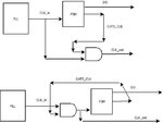
Diagram1.jpeg
First design:

Signal CLK_in is 120 MHz from PLL. It goes to to FSM module that generates serial data signal DO to external device with 4.3 ns setup and 0 ns hold time referring to clock signal ( CLK_out that has to be gated -- ( gated by signal from FSM register driven by CLK_in signal).

i guess that
Code:
derive_pll_clocks -create_base_clocks
derive_clock_uncertainty
create_generated_clock -name CLK_out -source [get_pins {inst6|pll_inst|altera_pll_i|CLK_in}] [get_ports {CLK_out}]
set_output_delay -clock { CLK_out } -max 4.2 [get_ports {DO}]
set_output_delay -clock { CLK_out } -min 0 [get_ports {DO}]

is not enought.

Second design is much worse idea -> clock is gated before FSM.
 

Is there a particular reason why you are using an AND gate instead of something like a BUFGMUX? Not only does that make the design a bit cleaner IMO, but I suspect it's easier to manage the constraints as well.

- - - Updated - - -

Oh wait, I see you are using Altera. Well, same question, but then with the Altera equivalent for clock muxes.
 

Yeah it can be and should be BUFGMUX for 2nd example. But as a practise, how to write proper constraints for mux and lut output clock.
 
Last edited:

In the 2nd case if the FSM controls the and gate. How does the FSM turn the clock back on as it will no longer run after the clock shuts off.

Using clock circuits like this are the worst idea you can have in an FPGA. I don't generate clocks like this in an FPGA. If I need a clock that I can enable/disable I use an XOR of phase shifted toggle FF outputs.

You probably should have asked this in the ASIC area as low power ASICs all deal with clock gating.
 

Code:
In the 2nd case if the FSM controls the and gate. How does the FSM turn the clock back on as it will no longer run after the clock shuts off.
It's one time wonder - FSM configures the external device at power up then its shuts off as it will never be turned again.
I know 2nd example is really bad, its just theoretical question how to make a proper constraints on this example ;]

Ok
Lets say we got external device without CS pin ( or tied to gnd) and we want to configure it once. Since CS is tied we cant apply there continous clock. So we created code that infer as example n1. Now what are the propper constraints.?
 

The only consumer of this gated clock is external? In that case you could use an ODDR with clock enable. No need for clock muxes.
 
  • Like
Reactions: axcdd

    axcdd

    Points: 2
    Helpful Answer Positive Rating
Even version 1 suffers from the following unless you've implemented opposite edge clocking:

Capture.PNG
 
  • Like
Reactions: axcdd

    axcdd

    Points: 2
    Helpful Answer Positive Rating
I guess i could easily take additional 180* shifted clock from PLL.
My main concern is that output clock is a clock signal that goes through some logic that will apply delay to it, that will count towards Th, Ts of external device. I doubt that
create_generated_clock -name CLK_out -source [get_pins {inst6|pll_inst|altera_pll_i|CLK_in}] [get_ports {CLK_out}] for muxed clock will inform fitter to take that delay into consideration for calculating output max/min delay. Or am i wrong ?
 

I guess i could easily take additional 180* shifted clock from PLL.
Altera FPGAs can use a local inversion of the clock...always @ (negedge clk) or if falling_edge(clk) then

axcdd said:
My main concern is that output clock is a clock signal that goes through some logic that will apply delay to it, that will count towards Th, Ts of external device. I doubt that
create_generated_clock -name CLK_out -source [get_pins {inst6|pll_inst|altera_pll_i|CLK_in}] [get_ports {CLK_out}] for muxed clock will inform fitter to take that delay into consideration for calculating output max/min delay. Or am i wrong ?
A gated clock shouldn't need to use create_generated_clock, create_generated_clock is used to generate clocks that can not be determined from propagating the clock. e.g. Toggle flip flop outputs used as divide by 2 clocks generators. You should probably look at the literature for source synchronous constraints. There is a good document that was written by an Altera guru about writing SDC constraints you should be able to find on Altera's user forum.

The clock in your case should propagate through the AND gate and will add to the clock network delay. It's still bad practice to add gates in the clock path as the clock path to the LUT is not a dedicated path and will vary depending on placement and routing. We've already given you a couple of possible improved solutions.
1. mrflibble's - use a ODDR register to generated the clock, will have consistent results and won't vary timing.
2. ads-ee - generate the clock using an XOR and two toggle flops that can be enabled/disabled that are 90% out of phase of each other. i.e. generate one on rising_edge clk and the other on falling_edge clk, you definitely want to use a 50% duty cycle input clock. This only makes sense if you need to also use the clock internally besides externally.
 
  • Like
Reactions: axcdd

    axcdd

    Points: 2
    Helpful Answer Positive Rating
See below for a quick example on how to hook up the DDR output register. This will implement your first version (upper one in your diagram).


Code Verilog - [expand]
1
2
3
4
5
6
7
8
ODDR gated_clock_out (
    .Q  (CLK_out),
    .C  (CLK_in),
    .CE (GATE_clk),
    .D1 (1'b1),
    .D2 (1'b0),
    .R  (1'b0),
    .S  (1'b0));


Quick reference for ODDR primitive, so you know what I'm on about: **broken link removed**

I kept the same signal names as in your diagram so you know what's what, but I suggest you rename them to something more sensible. For example, GATE_clk and CLK_in are a bit of a misnomer. I conveniently left out the parameters for the various modes, since you are using Altera. So you will have to use Altera specific primitives, but the above DDR output usage hopefully illustrates the idea. And you can use the same kind of ODDR for your DO signal. That will take care of skew and such.

PS: if you need to invert the clock output you can just swap the signals that are connected to D1/D2.
 
  • Like
Reactions: axcdd

    axcdd

    Points: 2
    Helpful Answer Positive Rating
Status
Not open for further replies.

Part and Inventory Search

Welcome to EDABoard.com

Sponsor

Back
Top