asimlink
Full Member level 1

- Joined
- Jun 24, 2009
- Messages
- 96
- Helped
- 12
- Reputation
- 24
- Reaction score
- 12
- Trophy points
- 1,288
- Location
- Islamabad
- Activity points
- 2,288
Hi,
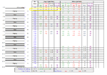
I am doing a board around xilinx virtex7 fpga in which i need to rout traces for upto 10~15Gbps GTH interfaces. I was looking through the pcb trace width and other parameters defined in xilinx virtex-7 evaluation board (V707) pcb stack [1].
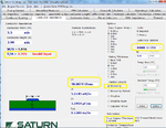
And I am using saturn pcb toolkit to compute characteristic impedance for single ended trace. But i get error that suggests T/H is an invalid input. Please refere to image [2] to see this error message produced by saturn toolkit.
I am doing this excercise as I need to change the material to Megtron-4 for my pcb and I offcourse need to adjust trace widths for single ended and differential signals for my design. Before actually doing this i wanted to validate the pcb trace width, clearance, heigh and copper widths used in Xilinx Virtex 7 (707 Evaluation board) .
Questions:
1. Can someone suggests if the pcb stack defined for v707 board is correct, then why saturn tool kit gives T/H error?
2. The characteristic impedance shown in xilinx pcb stack document says for 5.5mil single ended signal, the Z0 is 50 ohms, however
the calculated result by saturn toolkit shows it 40ohms?
3. Am I missing anything else, Although I have correctly selected the material Nelco 4000 EPSI from the list in Saturn PCB toolkit.
[1] Attached please see following pcb stack picture which is for xilinx virtex 7 evaluation board V707:
[2] Saturn pcb toolkit error message picture:
Regards
I am doing a board around xilinx virtex7 fpga in which i need to rout traces for upto 10~15Gbps GTH interfaces. I was looking through the pcb trace width and other parameters defined in xilinx virtex-7 evaluation board (V707) pcb stack [1].
And I am using saturn pcb toolkit to compute characteristic impedance for single ended trace. But i get error that suggests T/H is an invalid input. Please refere to image [2] to see this error message produced by saturn toolkit.
I am doing this excercise as I need to change the material to Megtron-4 for my pcb and I offcourse need to adjust trace widths for single ended and differential signals for my design. Before actually doing this i wanted to validate the pcb trace width, clearance, heigh and copper widths used in Xilinx Virtex 7 (707 Evaluation board) .
Questions:
1. Can someone suggests if the pcb stack defined for v707 board is correct, then why saturn tool kit gives T/H error?
2. The characteristic impedance shown in xilinx pcb stack document says for 5.5mil single ended signal, the Z0 is 50 ohms, however
the calculated result by saturn toolkit shows it 40ohms?
3. Am I missing anything else, Although I have correctly selected the material Nelco 4000 EPSI from the list in Saturn PCB toolkit.
[1] Attached please see following pcb stack picture which is for xilinx virtex 7 evaluation board V707:

[2] Saturn pcb toolkit error message picture:

Regards
