james.smith
Newbie level 4

- Joined
- May 11, 2013
- Messages
- 6
- Helped
- 0
- Reputation
- 0
- Reaction score
- 0
- Trophy points
- 1,281
- Activity points
- 1,336
Hi all,
New here, recently discovered the resource.
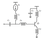
I have a question about biasing a common-emitter amplifier on-chip. I've done a good few audio amplifiers with op-amps or discrete transistors, and there a four-resistor network works well.
However, I've now started working with Cadence for M.Eng research, and I've been trying to get a simple CE amplifier designed. My question is, how does one bias it properly? I've got the Grey, Hurst, Lewis and Meyer book which I've completed, and it talks quite extensively about current sources and active loads, which I guess would be good to set the collector current, but how does one ensure that the transistor has the correct base-emitter voltage? Most of the book looks at such amplifiers from an ac perspective and omits biasing circuitry.
I've googled and searched library books but everyone seems to assume it's obvious and doesn't talk about it.
Thanks in advance for the help!
James


