Continue to Site

Welcome to EDAboard.com

Welcome to our site! EDAboard.com is an international Electronics Discussion Forum focused on EDA software, circuits, schematics, books, theory, papers, asic, pld, 8051, DSP, Network, RF, Analog Design, PCB, Service Manuals... and a whole lot more! To participate you need to register. Registration is free. Click here to register now.

Common Emitter amplifier base current

Status
Not open for further replies.

Resistanceisfutile

Member level 4
Member level 4
Joined
Aug 22, 2012
Messages
77
Helped
2
Reputation
4
Reaction score
1
Trophy points
1,288
Visit site
Activity points
2,008
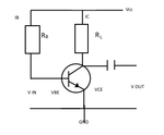
CEAmplifierDiagram.png
Ok so I have a really simple Common Emitter amplifier (I know it's not a very reliable circuit, but please ignore that).

I'm a little confused as to how I select the base current.

I have the equations: Vcc=IB*RB +VBE
and VCC=IC*RL + VCE

The component values are select so that IB makes VCE half the power supply voltage.
This is probably really simple, but can anyone help me out here? I'm confused as to how I select the right values.

Oh yeah, and the transistor VBE=0.6v, and hFE = 100
 

Work backwards from the output,
Vcc/2=Ic*RL
Ib=Ic/hFE (crudely, hFE varies w/ Ic)
Vbb=IB*RB+Vbe(Ib) (again, Vbe varies, ignore for analysis)
RB=(Vcc-Vbb)/Ib

badda-bing.
 

You NEVER EVER make a common-emitter amplifier like that. The base current for one transistor part number has a wide range (the hFE value) so some transistors will be saturated (high hFE) and other transistors will be cutoff (low hFE).
Negative feedback is needed to effectively reduce the range of hFE and to reduce the distortion. An emitter resistor and a voltage divider for the base can be used for negative feedback or the base resistor can be connected to the collector and the based fed from a fairly high impedance source.

The Vbe for one transistor part number is also a wide range. Some have a fairly low voltage (0.55V) and others have a fairly high voltage (0.75V).
 

How can anybody ignor the very basics of biasing a transistor??
I forgot to mention the problems caused by temperature changes on the very unreliable circuit.
 

How can anybody ignor the very basics of biasing a transistor??
I think, in this case we must discriminate between (a) designing a workable amplifier stage and (b) learning basic transistor properties based on idealized parameters.
More than that, such a non-reliable stage is a good starting point to show by calculation why stabilization of the dc operating point (negative feedback) is necessary.
This is a proven educational concept.
 

There are many teachers, books and tutorials about the very simple task of designing a workable common-emitter transistor circuit.
The workable circuit designs should be learned first because they show the problems caused by using the wrong design. The wrong design should not be learned first.

In his first post the OP stated the impossible conditions of a fixed Vbe and fixed hFE. A transistor part number should have been stated instead and the ranges of Vbe and hFE from the datasheet should have been shown and considered in the design.
It would have been simple to calculate biasing errors caused by having a transistor with a minimum and maximum Vbe and hFE in the wrong design and how negative feedback reduces the errors. The datasheet also shows the effect of temperature changes on the spec's.
 

Status
Not open for further replies.

Similar threads

Part and Inventory Search

Welcome to EDABoard.com

Sponsor

Back
Top