fobos3
Newbie level 6

- Joined
- Dec 25, 2010
- Messages
- 11
- Helped
- 0
- Reputation
- 0
- Reaction score
- 0
- Trophy points
- 1,281
- Activity points
- 1,335
Hi,
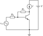
I am trying to design a common emitter amplifier with a current mirror for active load for an AGC. The problem I am having is that the voltage at my base is 0.7V + Vin. This causes a voltage offset when using small gain and saturation when using large gain, which is specified by the feedback network. Any ideas on how to solve this?
Regards
P.S.
Gain between Vb and Vout is about 59dB


