Continue to Site

Welcome to EDAboard.com

Welcome to our site! EDAboard.com is an international Electronics Discussion Forum focused on EDA software, circuits, schematics, books, theory, papers, asic, pld, 8051, DSP, Network, RF, Analog Design, PCB, Service Manuals... and a whole lot more! To participate you need to register. Registration is free. Click here to register now.

Clock issue on FPGA/DAC interface

Status
Not open for further replies.

e-potis

Newbie level 4
Newbie level 4
Joined
Sep 8, 2008
Messages
5
Helped
0
Reputation
0
Reaction score
0
Trophy points
1,281
Visit site
Activity points
1,330
Dear all,
This is probably not the right forum to post my issue, but it is seemed to be the most relevant.

I am interfacing a Xilinx ML506 board with a texas instrument parallel TI DAC evaluation board using a breakout board I designed. Both boards have header rows which I match on my pcb.

I am having issues with clock to the DAC, which I run at 275MHz,but have tried lower frequencies. It has a phase difference of 180 to the data lines, but I have tried all 90 degrees variations. The output of the DAC has phase noise at best and looks random at worst. I know it's the clock because I have found a way around the issue -getting a differential clock output and then converting it using an LVDS to CMOS converter - and it works fine. Also random trickery like putting a cap between the clock and ground sometimes work.

I have the Digital and Analogue supplies shorted on the DAC boards and it's powered from the FPGA board. My constrain for the clock is | IOSTANDARD=LVTTL | DRIVE=12 | SLEW = FAST;

Any solutions/ideas/clues would be greatly appreciated, as this is baffling me for quite a while now. I can provide schematics, scope grabs and any other kind of data you think could help you help me.

Thank you in advance
George
 

Hi,

275 MHz for a LVTTL clock seems a bit high.

With that high frequency the GND of both boards have to be connected plane to plane with very short (and best many) wires.

I picture of your application could help.

Klaus
 

Dear Klaus,
Thank you for your reply. I am aware that 275MHz is borderline fast for single ended signals. But the boards are rated (I am using an evaluation board for a 275MSPS DAC) for these speeds so they should in theory work. I have links to both boards in the original post.

There are more than 24 ground connections between the boards.

I should also add that there is a 50ohm resistor to ground on the DAC board near the clock input - which I have better luck when I remove. I don't understand why if I replace this with a nF range cap - the dac seems to accept the clock and works fine.

Thank you!
 

Hi,

I'd avoid these capacitors.
Did you use the clock_return signals to sample the data in your fpga?
I know it's not easy, but did you measure the signals and timing with scope. It's difficult because the scope's probe may cause more distortions than the lines itself.

Good luck
Klaus
 

I have found a way around the issue -getting a differential clock output and then converting it using an LVDS to CMOS converter - and it works fine.
Why don't you use this profound way to distribute a high speed clock signal? It would be my first choice anyway.

I agree that you'll preferably monitor the clock signal quality with an oscilloscope. But you need >= 1 GHz bandwidth and resistive dividers or active probes to get a halfway undistorted signal.
 

@Klaus I would avoid using the caps if I could find a better solution. I am sorry but I don't understand what you mean clock_return. Do you mean the negative edge? The clock that goes to the DAC is 180 to the one that drives the logic (and samples). I've also tried 90 and 270 degrees offset with not much success.

@FvM this is what I've been doing so far, but i consider it to be an elegant solution. I am getting the differential clock from the SMAs on the ML509. Ideally I'd like to run everything off the header rows. Plus, it frustrates me that I don't know what's wrong.

I will come back with the oscilloscope grabs you suggested later today.
Thank you both for your input.
 

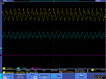
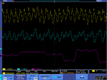
As promised... These were captured at 1GHz using the TPP1000 (1 GHz , 3.9pF / 10 MOhm) probes

01_init.png
System startup - only clock output (no instruction to generate samples). Yellow trace = clk FPGA side, Cyan = clk DAC side. Big difference.

02_run_no_cap.png
While also sending samples (purple line= DAC out). Terrible clocks

03_run_cap.png
With a capacitor between clock and ground on the DAC clock. Fairly good DAC output.

04_clk_vs_data.png
Here clk is yellow, data is cyan (LSB)

05_dclk_vs_data.png
The same, but with the clk cable detached (no clk input to the dac). Note that I had to change the scale.

Do these make any sense to you?
Again thank you for your time.
 

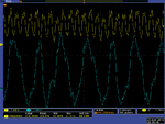
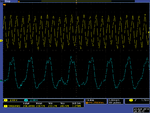
Update: I used a different FPGA output pin - different bank - and got a slightly better clock.


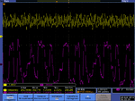
tek00000.png
Without a capacitor
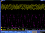
tek00001.png
with a cap
unnamed.jpg

But I still understand why the cap changes the clock in this way and if whether this is a valid solution.
 

A 275MHz single ended logic signal is going to be very hard to get across two pin headers. The differences in your results is probably just dumb luck with different impedance transformations on the clock path. Also keep in mind the phase of the clock relative to the other signals, which affects your SU/H times.
 

Status
Not open for further replies.

Part and Inventory Search

Welcome to EDABoard.com

Sponsor

Back
Top