Continue to Site

Welcome to EDAboard.com

Welcome to our site! EDAboard.com is an international Electronics Discussion Forum focused on EDA software, circuits, schematics, books, theory, papers, asic, pld, 8051, DSP, Network, RF, Analog Design, PCB, Service Manuals... and a whole lot more! To participate you need to register. Registration is free. Click here to register now.

clk generation based on control - reg

Status
Not open for further replies.

vinodkumar

Full Member level 5
Joined
Oct 5, 2006
Messages
251
Helped
12
Reputation
24
Reaction score
3
Trophy points
1,298
Location
hyderabad
Activity points
2,822
dear all,
iam looking for a verilog code :
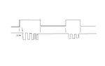
in which the input control signal is a signal with pulse width of 1us and period of 10us,
output signal should be logic 1 when control is zero and
40MHz clock when control signal is logic1 and clk should be assigned after 12.5ns of logic1 .
attached figure :

module(clk,control,latch_en);
input clk;//40MHz
input control;
output latch_en;
 

Attachments

  • 1.JPG
    1.JPG
    9.5 KB · Views: 75

The description is not clear. Please redefine the requirement in understandable way.
 

module test(clk, control, latch);
input clk;
input control;
output reg latch=0;

always @(control or clk)
begin
if(control == 1'b0)
begin
#12.5;
latch = 1'b1;
end
else
begin
#12.5;
latch = clk;
end
end


endmodule
test.jpg
 

i am looking for a syntheziable code
Yes, this could be assumed. There are two points:
- you need an input clock to your design
- if we presume, that the input clock is unrelated to the control signal, you can't easily achieve a fixed delay between control signal and output clock.

You can approximate the intended 12.5 ns delay by using a higher input clock or multiplying it with a PLL and divide it down, synchronized to the control signal.But the delay won't be exact.
 

But the delay statements don't work in synthesis.
Yes sir, you are right. Now an actual hardware delay can be introduced by the use of counter. I will try that.
 

already i have shown the clock as an input which is 40MHz,but it is not synchronous with control signsl...

i am having an approach
where in 80MHz clock is generated using DCM and
12.5ns delay obtained from risisng edge of control signal
1's and 0's are stored already in a ROM,
they will be read for alternate count of 80MHz clock....
here exact delays are possible i think...
but i am looking for better approach...


regards,
vinod kumar...
 

here exact delays are possible i think...
Delay of an asynchronous signal will be always inaccurate by an amount of a clock period at maximum. Presuming your FPGA has high frequency PLLs ("DCM"), you can multiply the clock frequency and reduce the delay error, as adresses in post #6. You can even create multiple phase shifted clock and select the best one on the fly. Or use logic cell delay chains in combination with the clock. It ends up in a rather complex design anyway.
 

Stupid question: what is this used for, and how precise must this 12.5 ns delay be?
 

Status
Not open for further replies.

Part and Inventory Search

Welcome to EDABoard.com

Sponsor

Back
Top