DrBudz
Junior Member level 3
Hi folks,
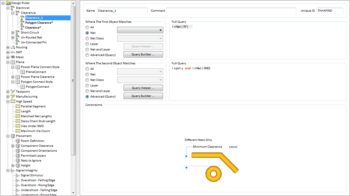
I have one RF trace which requires 12mil clearence. Other components and nets have 10mil clearence.
I want to place ground plane which will have 14mil clearence on the whole board, except near the RF trace where it should be 12mil.
How can I make the clearence between ground plane and RF trace to 12mil and between ground plane and rest of the traces to 14 mil?
Is there samo sintax like this:
clearence between GND_Plane and RF_Trace = 12mil
clearence between GND_plane and Other_traces =14mil
Thanks