Continue to Site

Welcome to EDAboard.com

Welcome to our site! EDAboard.com is an international Electronics Discussion Forum focused on EDA software, circuits, schematics, books, theory, papers, asic, pld, 8051, DSP, Network, RF, Analog Design, PCB, Service Manuals... and a whole lot more! To participate you need to register. Registration is free. Click here to register now.

Class E using MOSFET as swicth gives Non-zero voltage in ON state

Status
Not open for further replies.

zopeon

Member level 2
Joined
Sep 12, 2008
Messages
51
Helped
7
Reputation
14
Reaction score
2
Trophy points
1,288
Location
India
Activity points
1,612
Hello everyone,
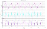
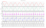
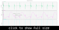
I have to design a class E output stage for Pout= 8mW (targeted for zigbee type apps ) with fc = 2.45Ghz using UMC 180nm RFCMOS technology. I have gone through RF books by Lee and Crips and through Sokal et all Class E paper. but when I designed it and ran transient analysis I get the On-state voltage closer to the Vdd (1V) what am I doing wrong?
Also could you guide me any other material to help me in my design?
other doubts are
Ropt value for this comes greater than 50 is it correct??
Selection of MOSFET size as it is to be used as a switch?


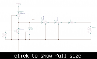
I am using cadence spectre for simulation
Thanks & Regards
 

The load resistance for this design is 72.1 ohm. you should consider the dissipations. For 100% efficiency circuit draw 8mA from 1v DC supply but taking the dissipations in account this value is greater. The circuit component values are shown in the attached figure. By the way as for class-e PAs with RF choke, the feed inductance value should be greter than 10R/2*Pi*f, where R is load resistance and f is opperation frequency, then for your one this value exceeds 46nH. For design with finite DC feed inductance refer to:
Acar, M.; Annema, A.J.; Nauta, B.; , "Generalized Design Equations for Class-E Power Amplifiers with Finite DC Feed Inductance," Microwave Conference, 2006. 36th European , vol., no., pp.1308-1311, 10-15 Sept. 2006.


thanks Masoud180,
I am referring the same paper for finite dc-feed inductance.
Problem is with getting sufficient values for L0 and c0 with Ql(loaded Q) = 3 or more.
eg. If I set Ql = 3, and R = 72 and I get l0 = 14nH which is manageable but C0 = 0.3pF is too low. at 2.45Ghz. Also I should size the MOSFET such that the current Id is 8mA or more in linear region, right? Wouldnt the finite dc-feed inductance cause more current to flow (current fluctuations) with average closer to the desired value? Will we have to decide the MOSFET size after the L,C,R values are determined as these values would affect the current through it, is it right?
thanks
 

I think there are some design errors because the waveforms don't seem to be correct to me ...
For instance, choke coil value should be higher than 1.7nH for 2.45GHz.And so on..
The current waveform is absolutely not correct, it should been sinusoidal-like because the drain current does not increase instanteanously..
Check the component values double..

Actually the choke should be 46nH for R = 72 (required power and Vdd) The problem is due to use on finite dc-feed inductance the drain current is not constant.
 

Zopeon, As I know the MIM capacitance in 0.18um TSMC standard design is in femtofarad range, so there is no problem with 0.3pf capacitance. But remember that original class-E components value introduced in literatures are valid for designs for output filters with quality factor more than 10. So for quality factor of 3, you must compute components differently. For it refer to:
Hung-Lung Tu, S.; Toumazou, C.; , "Effect of the loaded quality factor on power efficiency for CMOS class-E RF tuned power amplifiers," Circuits and Systems I: Fundamental Theory and Applications, IEEE Transactions on , vol.46, no.5, pp.628-634, May 1999.

Of course for the low quality factors, you must consider high distortion due to harmonics. The Y1 plot seems to the transistor's current. But as the current through the transistor is the sum of drain-source capacitance(which make a part of parallel capacitance) and the transistor current, it does not give you a good view. So it is better to plot the current through C36 and transistor current, which is sinusoidal.
Peak current through the transistor is 2.84Idc (RF power amplifiers by Kazimierczuk). so the transistor must sustain this current. The only matter with transistor size is the On-state resistance of the transistor, that decreases when the transistor size increases. But how much can the size increase? When you increase the transistor size, the input capacitance of the transistor increase, so you should mind the input power which lower "power added efficiency" (PAE=(Pout-Pin)/Pdc). You should design the circuit and compute load-network components value, and then increase the transistor size and optimize the PAE of your circuit. I attach a photo to show an example of the changes of efficiency and PAE when transistor fingers incrase. The transistor size of RF-MOS transistors of TSMC are limited, so this transistor is not suitable for power application, I guess you may have to choose standard one.
For DC-feed inductance, the fluctuation of the current flowing through it is not negligible comparing to DC value of it, but the average of the current is constant ( for a given DC supply and output power). The fluctuation of the current can not be absolute-zero, since ideal RF choke is not available.

 
Last edited:
  • Like
Reactions: zopeon

    zopeon

    Points: 2
    Helpful Answer Positive Rating
Zopeon, As I know the MIM capacitance in 0.18um TSMC standard design is in femtofarad range, so there is no problem with 0.3pf capacitance. But remember that original class-E components value introduced in literatures are valid for designs for output filters with quality factor more than 10. So for quality factor of 3, you must compute components differently. For it refer to:
Hung-Lung Tu, S.; Toumazou, C.; , "Effect of the loaded quality factor on power efficiency for CMOS class-E RF tuned power amplifiers," Circuits and Systems I: Fundamental Theory and Applications, IEEE Transactions on , vol.46, no.5, pp.628-634, May 1999.


Of course for the low quality factors, you must consider high distortion due to harmonics. The Y1 plot seems to the transistor's current. But as the current through the transistor is the sum of drain-source capacitance(which make a part of parallel capacitance) and the transistor current, it does not give you a good view. So it is better to plot the current through C36 and transistor current, which is sinusoidal.
Peak current through the transistor is 2.84Idc (RF power amplifiers by Kazimierczuk). so the transistor must sustain this current. The only matter with transistor size is the On-state resistance of the transistor, that decreases when the transistor size increases. But how much can the size increase? When you increase the transistor size, the input capacitance of the transistor increase, so you should mind the input power which lower "power added efficiency" (PAE=(Pout-Pin)/Pdc). You should design the circuit and compute load-network components value, and then increase the transistor size and optimize the PAE of your circuit. I attach a photo to show an example of the changes of efficiency and PAE when transistor fingers incrase. The transistor size of RF-MOS transistors of TSMC are limited, so this transistor is not suitable for power application, I guess you may have to choose standard one.
For DC-feed inductance, the fluctuation of the current flowing through it is not negligible comparing to DC value of it, but the average of the current is constant ( for a given DC supply and output power). The fluctuation of the current can not be absolute-zero, since ideal RF choke is not available.


can you show me the expected power transient waveform for finite dc-feed inductance class E PA?
thanks
 

Here is my own design. The transient response of Class-E PAs with finite-DC feed inductance are faster than those with RF chock, so make them more suitable for "envelope elimination and restortion" technique.


Obviously, the main difference between both circuits is in transistor sizing.
 

Here is my own design. The transient response of Class-E PAs with finite-DC feed inductance are faster than those with RF chock, so make them more suitable for "envelope elimination and restortion" technique.

thanks a lot, could you show the vout waveform also, i have doubt in it.
i am getting the following waveforms.
 

Attachments

  • pa2.png
    pa2.png
    26.7 KB · Views: 125
Last edited:

Take a look on the out waveform. If it seems to be distorted, because the quality factor is low.


thanks a lot, So my Switching waveforms seems ok, right? if you neglect the non-zero On voltage. I could not reduce it without degrading the PAE to unsuitable level. As with increased size ( reduced Ron) the current increases. I am also getting a distorted sine wave. So what should be the minimum Ql for non distorted value? If I am using constant amplitude modulation scheme is it ok if there is distortion? or will it also affect the phase of signal?
Thanks for your help!
 

The waveforms are OK but the bounces are unusual. One thing you should remember, the transistor operates in ohmic or cutoff region. So the current does not depent on the transistor size. The current of the transistor is dictated by the feed-inductance current and output current. So if you increase size of transistor, you can reduce drain-source voltage when transistor operates in ohmic region. maximum distortion level of the output signal depends upon your application. The harmonic level of the output is for example -60dm relative to carrier signal in some RF telecommunication application. Nominal quality factor for the output resonance filter is 10. If you want to increase it, then bigger inductance is needed which present more parasitic resistance and therefore reduces the efficiency. The phase of the output carrier signal depends on the excessive inductance in serie with resonance circuit, so you should not worry about phase of the carrier signal. Of course output signal distortions are due to harmonics added to the carrier signal, not the phase distortion.
 

Thanks,
Could you please explain, How to reduce the Vds, So as to achieve a current flow of about 9mA through the dc-feed inductance and still use MOSFET of 840µm. I cannot see any way of increasing the Ql without decreasing the Load R.( As L0 and C0 are at boundry values for UMC implementation) Also the calculated value of L dc-feed inductance comes to be 1nH for R= 22 ohms using the Nauta paper(same as given by you). Also we have to first do transient analysis to get the waveform or some other analysis??
Thanks
 

According to ohm's law, Vds=Ron*Ids, so the only way to reduce the drain-source voltage in ohmic region is to increase the transistor size. When the transistor is off, peak of Vds is 3.56 Vdd. So designers must be careful of gate oxide breakdown phenomenom. If the inductors value of UMC technology is limited, if guess you can reach your desired value using series of inductors. OF course how much this is reasonable, I do not know. As I know, implementing inductors using bond wires is possible in nanohanry range and they are used as feed-inductance regularly. These inductors offer high quality factor.
 

But if I increase the width, Id increases and Vds remains constant. How to ensure Id remains constant with increased width for finite dc-feed inductance. How do you estimate the MOSFEt capacitance? I run dc analysis with the sitch in cut-off state and see the various cap values and use the formula C=(Cdd || Cds || Css ) + Cdb is this correct?
Thanks
I tried designing a Class E even Harmonic PA, and I am getting the required waveform. I get my output voltage and current at 2.5GHz (expected) When I see the dft of output voltage I get a lot of harmonic distortion. I had taken Ql = 10 , How to check the actual Ql?
 

Attachments

  • PA_E_evenHarmonic_HP.png
    PA_E_evenHarmonic_HP.png
    40.2 KB · Views: 163
Last edited:

Status
Not open for further replies.

Part and Inventory Search

Welcome to EDABoard.com

Sponsor

Back
Top