Continue to Site

Welcome to EDAboard.com

Welcome to our site! EDAboard.com is an international Electronics Discussion Forum focused on EDA software, circuits, schematics, books, theory, papers, asic, pld, 8051, DSP, Network, RF, Analog Design, PCB, Service Manuals... and a whole lot more! To participate you need to register. Registration is free. Click here to register now.

Charge Pump, Problem with diode

Status
Not open for further replies.

ata90

Member level 5
Member level 5
Joined
Apr 13, 2009
Messages
89
Helped
1
Reputation
2
Reaction score
1
Trophy points
1,288
Visit site
Activity points
1,945
Dear all

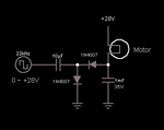
In order to run 48V, 0.6A motor with 24V power supply, I implemented circuit bellow which used charge pump and generated negative voltage. the voltage around the motor is near to 48V and motor works properly; but the problem is that both of 1N4007 diodes become too hot. is it the nature of these diodes to become hot at this current?
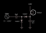
Charge Pump.PNG

Thanks for any helps..
 

Attachments

  • Charge Pump.PNG
    Charge Pump.PNG
    3.8 KB · Views: 174

22 kHz operation of slow reverse recovery diodes will involve a lot of switching losses. Peak current of the voltage doubler is > 1.2A and cause increased forward losses. I would use 3A/40V schottky diodes.
 
Thanks for your helpful reply..
Is it good idea to decrease switching frequency? or the only solution is to use schottky diode?
 

Lower switching frequency requires larger capacitors. 1N4007 is good up to a few kHz, peak currents still suggest 2 or 3A diodes.
 
I believe I recognize Falstad's simulator, looking at your schematic.

That's the same one I normally use. I seem to enjoy experimenting with charge pumps and voltage doublers.

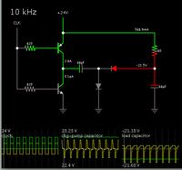
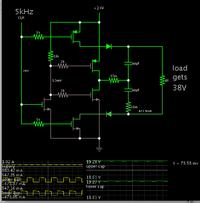
My simulation shows most every component carries 2.8 amperes at approximately 25% duty cycle.

This includes the charge-pump capacitor. 10 uF is liable to be small for carrying that much current.

I believe you could make each capacitor around 68 uF.

My screenshot, with scope traces:


@BradtheRad

1. How much is the breakdown voltage of that capacitor placed between transistor and diode?
2. I think the value of output capacitor is not enough. and maybe in practice you have ripple in output. isn't it?
3. Do you prefer 10KHz switching instead of 22KHz? why?
4. Because of inductive load, isn't it necessary to place freewheel diode at output?
5. The only problem of my circuit is what I mentioned before. if I replace 68uF capacitor and 10KHz switching in my circuit, then 1N4007 diodes don't become hot?
 

The maximum capcitor voltage can be easily seen, I think. It's 24 V for both capacitors.

Yes, the output capacitor should be large enough to hold the negative output voltage. Obviously 68 µF can't.

AC current rating of capacitors should be considered, too. No regular 10 µF (or 68 µF) electrolytic capacitor is designed to carry > 1 A rms.

As long as the load isn't switched, you won't need a freewheeling diode.

I'm under the impression that you don't believe what's been said about reverse recovery losses of slow diodes.
 
@FVM

About term 5, yes I know for 22 KHz switching, schottky diode is necessary. I thought maybe 1N4007 is suitable for 10 KHz switching. anyway..
AC current rating of capacitors should be considered, too. No regular 10 µF (or 68 µF) electrolytic capacitor is designed to carry > 1 A rms.
Which kinda capacitors have been designed to carry up to 1A?
 

Which kinda capacitors have been designed to carry up to 1A?
Special low ESR types, or larger capacitance (1000 µF or above) electrolytic capacitors. They also allow to reduce the switching frequency.
 
Some of your items were covered above, so I'm replying to the others.

2. I think the value of output capacitor is not enough. and maybe in practice you have ripple in output. isn't it?

I played with capacitor values until the simulation showed a few percent variation in volt levels on the capacitors.

When the charge-pump capacitor is too small a value, voltage at the load starts going down. It's not necessarily bad, since your load may not necessarily need the maximum volt level.

The simulation is only theory acted out, of course. It may be a far cry from reality.

3. Do you prefer 10KHz switching instead of 22KHz? why?

I was seeing how things behave with the larger size capacitors since they are recommended. By using larger capacitors it allows operation at a few kHz. That might allow you to get by with ordinary diodes (per post #4).

As we know there is an advantage to switching at frequencies beyond the range of human hearing.

I tend to use slower frequencies because Falstad's simulator has a limit to how fast the oscilloscope traces can travel.

5. The only problem of my circuit is what I mentioned before. if I replace 68uF capacitor and 10KHz switching in my circuit, then 1N4007 diodes don't become hot?

The diodes will still carry those large current pulses (regardless of the operating frequency). It is unavoidable with this charge pump topology as it must carry current bursts amounting to several times your desired load current.

The small diodes are carrying 700 mA average. Even though this is within tolerance for the 1N400x series, it is the form of current bursts of 2.8 A (estimated) at 25% duty cycle. This has to be a strain on them.

As for the 10 uF capacitor (the charge-pump) I would be surprised if it is not heating up. The important thing is for both capacitors to be physically large enough to handle 2.8 A going through one way and then the other.

The smoothing capacitor does not need to be so large as it would be this were a 60 Hz power supply. It can be of a smaller size, similar to if it were in a switch-mode power supply. However if you find 1000 uF stays cool, and reduces ripple sufficiently, then there is no need to reduce its value.

You can experiment with values yourself by clicking on the link below. It will open the falstad.com website, load my schematic and run it on your computer. (Click Allow to load the Java applet.)

I guess you know how to save layouts to disk.

https://tinyurl.com/czgjq6s
 
  • Like
Reactions: ata90

    ata90

    Points: 2
    Helpful Answer Positive Rating
Apart from the current rating problem, you are right that 68 uF is sufficient. I didn't read the waveform voltage range previously.
 
  • Like
Reactions: tpetar

    tpetar

    Points: 2
    Helpful Answer Positive Rating
BradtheRad and FVM, Thanks for your solution..

@BradtheRad, By the way, how did you upload your JAVA Applet schematic on the net?
 
Last edited:

Apart from the current rating problem, you are right that 68 uF is sufficient. I didn't read the waveform voltage range previously.

I'm not as careful as I ought to be about adding a label 'green trace=voltage' and 'yellow trace=current'.

- - - Updated - - -

@BradtheRad, By the way, how did you upload your schematic on the net?

The Falstad simulator has a command in the File menu called 'Export link'.

I would not have known when to use it, until I saw where a poster (here at edaboard) gave a link to his simulation. When I clicked it I saw the simulation begin to run on my screen. That's when I put 2 and 2 together.

As far as I know, Falstad's is the only simulator that does this.
 

Today I replaced 1N4007 diodes with schotkky diodes. there was no heat generated by circuit. Thanks alot for your solution.
I have another question, is there any ways to generate -12V instead of -24V from the positive power supply of +24V? in other word I have totally 36V p-p at output instead of 48V?

- - - Updated - - -

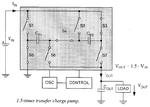
During my search through the papers, I could find this topology; however I don't know how it can be implemented.
Thanks for any suggestion

Charge Pump02.PNG
 

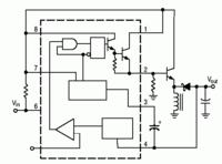
A "not-so-good" solution is to reduce the series capacitor value until it drops enough voltage. A better way is an inverting DC/DC converter using an inductor, with voltage regulation. You can e.g. refer to MC34063, a classical low-cost voltage converter chip, here is an application circuit from the datasheet.

 
I have another question, is there any ways to generate -12V instead of -24V from the positive power supply of +24V? in other word I have totally 36V p-p at output instead of 48V?

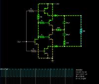
Here is a capacitor stack method I devised (in simulation).

I have not seen this schematic anywhere, and I don't know why. Could be because it is only 75 percent efficient.


It will work only if your load does not need the 24V ground reference. In other words, it must operate on the floating 38V from the capacitors.

I tried to get it to work with transistors, but it allowed unwanted current flows from the PNP bases down to the NPN bases.

The diodes are necessary to prevent upward current flows.

During my search through the papers, I could find this topology; however I don't know how it can be implemented.
Thanks for any suggestion

View attachment 83483

This would require 7 mosfets/transistors and a lot of work.

It is not too different from my method above, although it is probably more efficient.
 
  • Like
Reactions: ata90

    ata90

    Points: 2
    Helpful Answer Positive Rating
I simulated your schematic. I don't know what problem is with my schematic. but I couldn't achieve to desire result. the clock signal is 0 ~ 24V. look at picture below. I don't recognize any difference between your schematic and mine!
please export link or paste your code.


You've been fooled by the Falstad syntax, 10m(milli) isn't the same as 10M (Mega), in contrast to SPICE. 10m has to be entered as 0.01

The suggested circuit is essentially a voltage doubler with some losses. You can achieve the same by adding losses to your original cicruit, e.g. with a series resistor.
 
I simulated your schematic. I don't know what problem is with my schematic. but I couldn't achieve to desire result. the clock signal is 0 ~ 24V. look at picture below. I don't recognize any difference between your schematic and mine!
please export link or paste your code.

Yes, that's what I should have done.

https://tinyurl.com/bq2z96l

As FvM points out, the m-ohms is milli-ohms.

When I have used transistors, they conduct efficiently. Losses are small. The load can get as high as 45V.

By trying mosfets I found they conduct less efficiently. This automatically reduces load voltage. This effect may or may not show up in real hardware. I find that Falstad's simulation requires a higher gate voltage so the mosfet will conduct, than I have seen with real mosfets.
 

Status
Not open for further replies.

Similar threads

Part and Inventory Search

Welcome to EDABoard.com

Sponsor

Back
Top