Continue to Site

Welcome to EDAboard.com

Welcome to our site! EDAboard.com is an international Electronics Discussion Forum focused on EDA software, circuits, schematics, books, theory, papers, asic, pld, 8051, DSP, Network, RF, Analog Design, PCB, Service Manuals... and a whole lot more! To participate you need to register. Registration is free. Click here to register now.

charge pump bug, need help

Status
Not open for further replies.

crazyfox

Junior Member level 2
Joined
May 12, 2007
Messages
23
Helped
0
Reputation
0
Reaction score
0
Trophy points
1,281
Activity points
1,452
HI :

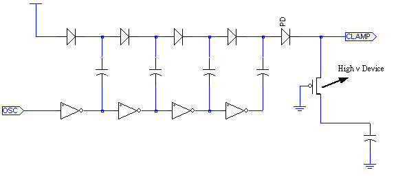
I have a charge pump circuit like Fig. , from the simulation result it can pump up

to the 12v , but in real measurement, i find the block cannot pump to the high

voltage. The question is it really hard to find the bug on the wafer, anyone who

have ever design the charge pump, can give me some suggestion from your

experience, which place that i might not concern. Any way could i find the

problem of the circuit on the wafer.

One that i can think is the HV device have leakage current, and the other is the

diode device might have problem, layout? or model? how to verification ?


Thanks for your read and give me suggestion
 

Where is the bulk of the HV device connected., Substrate leakage of this device is normally a huge concern.
 

The bulk of the HV device was connected to the clamp
 

All diodes have their own (isolated) well?
 

What if each diode were really a substrate-collector BJT?
That's a good way for small currents to go "down the rabbit
hole".

Think about it.

Then make sure you have not only proper well isolation,
but also that well ties are sufficient to keep not only DC
but the charge pump transients from waking up E-B
junctions.

It might help you to try drawing up the cross sections
for the circuit shown, and try to assign parasitic BJT terminals
and voltages as a check.
 

    crazyfox

    Points: 2
    Helpful Answer Positive Rating
Yes, all the diode have their own well .

Thanks for both of your suggestion.

dick_freebird, thanks for your detail suggestion, it gives me a way

to find out the bug of this circuit.
 

I agree with dick_freebird. What type of process are you using? Can you replace the PN diode with a schottky diode (The forward drop is low enough to prevent the pnp from activating)? Do you have a free NPN transistor available with a breakdown voltage > VDD? If yes then replace each diode with a zener connected npn(base shorted to collector). If not maybe you can use pmos transistors as diodes. Here you must leave the well floating, or you'll be in the same situation.
 

I also agree with dick_freebird. For general process, most of diodes were not allowed for forward-bias because of its parasite bipolar (NPN or PNP). Maybe you need special process with special ioslation (like N+ buried layer or other techniques) to reduce current-gain of parasite bipolar.
 

Status
Not open for further replies.

Part and Inventory Search

Welcome to EDABoard.com

Sponsor

Back
Top