Continue to Site

Welcome to EDAboard.com

Welcome to our site! EDAboard.com is an international Electronics Discussion Forum focused on EDA software, circuits, schematics, books, theory, papers, asic, pld, 8051, DSP, Network, RF, Analog Design, PCB, Service Manuals... and a whole lot more! To participate you need to register. Registration is free. Click here to register now.

Characteristic impedance of combination of CPWG and stripline on inner layers

Status
Not open for further replies.

simon.vdw

Newbie level 1
Newbie level 1
Joined
Jan 10, 2020
Messages
1
Helped
0
Reputation
0
Reaction score
0
Trophy points
1
Activity points
14
Hi everyone,

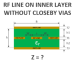
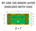
I have been searching for quite a while about the following subject, but can´t seem to find a decent answer on this. Imagine a 4-layer PCB (Top layer, Mid1 layer, Mid2 layer, Bottom layer). Mid1 layer and Bottom layer are GND panes with here and there vias to pass signals from the top layer to the Mid2 layer and back. RF signals on the top layer are done using CPWG. RF signals on the Mid2 layer are done with stripline or - and now comes the tricky part - striplines surrounded by GND planes as well. My question louds: What is the characteristic impedance of these kind of RF lines? Note that these kind of RF lines are no ordinary striplines, but rather striplines + surrounded by GND Planes at both sides, so similar to a CPWG, with GND plane also above the RF line. I have add two images to clarify.

Thanks and best regards
Simon
 

Attachments

  • RF line on inner layer without closeby vias.PNG
    RF line on inner layer without closeby vias.PNG
    15.3 KB · Views: 273
  • RF line on inner layer shielded with vias.PNG
    RF line on inner layer shielded with vias.PNG
    16.9 KB · Views: 156

FvM

Super Moderator
Staff member
Advanced Member level 7
Joined
Jan 22, 2008
Messages
51,209
Helped
14,651
Reputation
29,580
Reaction score
13,795
Trophy points
1,393
Location
Bochum, Germany
Activity points
292,720
The embedded CPWG (second picture) is covered by some calculation tools, e.g. Polar Si6000 and Si8000. Specific inductance and capacitance can be also calculated with 2D solvers like Quickfield Student.

Via fences are generally required to avoid unwanted wave modes, hence the point involved with figure 1 versus 2 isn't if you have vias but how close they are. The figure 1 vias are still in the coplanar ground "slipstream" and won't change impedance much. PCB thickness variations probably matters more.

If you want exact modelling of a specific PCB geometry, a general 3D solver or planar specific solver like ADS Momentum would be necessary.
 

volker@muehlhaus

Advanced Member level 5
Joined
Apr 11, 2014
Messages
2,907
Helped
1,039
Reputation
2,084
Reaction score
1,073
Trophy points
1,393
Activity points
18,725
Via fences are generally required to avoid unwanted wave modes

Yes exactly. By leaving out those vias, your various "ground" metals are unconnected and can be start to have unwanted potential here and there ... causing all sorts of resonance and strange behaviour. Then it's no longer "all ground" but instead all different conductors that are only connected somewhere far away. Don't do that!

You don't need to create a via fence, but make sure all grounds are connected at distances closer than lambda/10 wavelength (wavelength in PCB medium, not air)
 

Status
Not open for further replies.

Part and Inventory Search

Welcome to EDABoard.com

Sponsor

Top