Continue to Site

Welcome to EDAboard.com

Welcome to our site! EDAboard.com is an international Electronics Discussion Forum focused on EDA software, circuits, schematics, books, theory, papers, asic, pld, 8051, DSP, Network, RF, Analog Design, PCB, Service Manuals... and a whole lot more! To participate you need to register. Registration is free. Click here to register now.

Cascade amplifier: producing wrong frequency at second stage

Status
Not open for further replies.

ahamshubham

Junior Member level 1
Joined
Jun 7, 2013
Messages
15
Helped
1
Reputation
2
Reaction score
1
Trophy points
1,283
Visit site
Activity points
1,383
I am building a receiver circuit which receives a signal of approximately 3.6MHz. The signal received is of very low amplitude (5mV) so I had to use an amplifier. When I couple the input to a single BC547B amplifier, the output becomes an amplified version of the signal around 50mV. But, when I connect another BC547B amplifier, the circuit produces an unwanted frequency at the output. So, I kept a variable resistor at collector of the second transistor. The output seems to appear when my collector resistance (R8) is about 26ohm. For the remaining resistor values, there are unwanted frequencies at the output. What is wrong with the second stage. Also, can someone suggest how to obtain the amplitude of this high frequency wave (I thought of using high frequency peak detector). Here is the link to the schematic and a picture of my circuit:

https://obrazki.elektroda.pl/2879148000_1427745135.png

https://obrazki.elektroda.pl/7595573400_1427744997.jpg
 

I'm no sure what the second link has to do with 3.6MHz amplifiers.

Your problem is instability. When you have high gain, particularly with an LC network in the circuit, any feedback will tend to make it oscillate. You need to be very careful of the layout, try to keep the output side away from the LC circuit. Also ensure the power and ground rails cannot conduct signal back to the first stage. I suggest you add one or more 100nF caramic capacitors between 9V and ground. If that doesn't stop it, connect the 9V directly to the second stage and add a resistor of say 100 Ohms in the supply to the first stage. Make sure you have a capacitor of 100nF and 10uF in parallel between the first stage supply (after the 100 Ohm resistor) and ground.

There is also no point in using large values for C1, C2 and C6, I suggest you drop them to 100nF.

Brian.
 
Your schematic had wires running around in circles (Multisim?). I fixed it.
Why did you reduce the collector resistor value of Q2 to be so low?
 

Attachments

  • 3.6MHz amplifier.png
    3.6MHz amplifier.png
    18.5 KB · Views: 134

I'm not sure what the second link has to do with 3.6MHz amplifiers.
Sorry, that was a mistake. Actually I wanted to send the picture in the attachment.

I suggest you add one or more 100nF ceramic capacitors between 9V and ground. If that doesn't stop it, connect the 9V directly to the second stage and add a resistor of say 100 Ohms in the supply to the first stage. Make sure you have a capacitor of 100nF and 10uF in parallel between the first stage supply (after the 100 Ohm resistor) and ground.
There is also no point in using large values for C1, C2 and C6, I suggest you drop them to 100nF.
So, my circuit after alterations based on your suggestions looks like this:
**broken link removed**

I will make the circuit and will tell you the results.

- - - Updated - - -

Your schematic had wires running around in circles (Multisim?). I fixed it.
Yes, it is a multisim simulation. Thanks for making it out neatly.

Why did you reduce the collector resistor value of Q2 to be so low?
The resistor was a variable one and when I reached 26 ohms, the amplified signal came. At other values, it gave different frequencies at the output. I will try it out again and will tell you for sure.

- - - Attachment- - -
 

Attachments

  • DSC_0169.jpg
    DSC_0169.jpg
    710.3 KB · Views: 124
Last edited:

In your prototype, move the second transistor away from the first and carry out the supply decoupling as suggested. It is a very basic sort of amplifier which should be stable. it could be worth examining your earth conductor, could be you have a bad joint somewhere.
Frank
 
Of course your circuit is a tangle of wires on a solderless breadboard. The capacitance between the many rows of contacts and between all the jumper wires causes high frequency loss and/or oscillation. A solderless breadboard should be used only for DC and low audio frequencies. Your circuit should be built on a pcb or a soldered compact stripboard layout.

Your electrolytic capacitors have a value much too high at 3.6MHz and they are inductive above a few hundred kHz. You do not want inductive capacitors at VHF frequencies. I do not see an important supply bypass capacitor.
The collector of the transistor on the left side is not connected to anything.
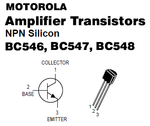
Did you look at the datasheet to see the pins on the transistors?
 

Attachments

  • BC547 pins.png
    BC547 pins.png
    12.4 KB · Views: 132
Your electrolytic capacitors have a value much too high at 3.6MHz and they are inductive above a few hundred kHz. You do not want inductive capacitors at VHF frequencies.
Okay, so I did not see your post. But either randomly or due to the fact betwixt posted that I should keep value of my capacitances near 100nF, I replaced the 47uF capacitance (C6 in your diagram) with a capacitance of 2.2uF. After that, my circuit started giving the required amplified output (amplitude nearly 1 volts). It now works at a collector resistance of 1kohm. But, there are still oscillations present (at a different frequency) with the output superimposed on them. Source decoupling did not help much in removing the oscillations (Although, I did not experiment with it that much after my output came). I think I will try and replace both bypass capacitors with 100nF capacitances.
Also, can you tell me why the capacitors will behave as inductors at this frequency?

Of course your circuit is a tangle of wires on a solderless breadboard. The capacitance between the many rows of contacts and between all the jumper wires causes high frequency loss and/or oscillation. A solderless breadboard should be used only for DC and low audio frequencies. Your circuit should be built on a pcb or a soldered compact stripboard layout.
My next attempt will be to build the circuit on a stripboard and I will place the results here.

The collector of the transistor on the left side is not connected to anything.
Not that dumb, man. It was connected to the variable resistor which I removed during taking the picture.
 

An electrolytic capacitor has its foil and insulation wound around and around inside it making it have inductance. A modern film capacitor has fairly low inductance. A ceramic capacitor has extremely low inductance.
At 3.6MHz a 2.2uF ceramic capacitor will have a reactance of only 0.1 ohms and its very small drop in voltage gain will be impossible to measure. A 0.1uf ceramic capacitor reactance is 0.4 ohms and its loss of voltage gain will also be impossible to measure.

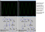
I simulated your first transistor using "perfect" capacitors that have no inductance (ceramic capacitors) and very short wiring that also has no inductance:
 

Attachments

  • Emitter capacitor.png
    Emitter capacitor.png
    55.5 KB · Views: 116
Found a different reason here:
**broken link removed**
Will use ceramic capacitors.
 

Ivan-Holm posted a reply (then deleted it) that a BC547 transistor "can only be used to LF signals :) see datasheet it has an A_bw =1MHz".
But the datasheet shows that it has a typical gain-bandwidth product of 300MHz. It is used frequently as the RF oscillator in a 100MHz FM transmitter.
 

A_bw is where the A is almost 1, it says typical 150Mhz and max 300Mhz, and yes I think of the opamp datasheet with A_bw. but see the datasheet it is 150Mhz. but I will never use only use it in LF, because it is a noise transistor. some like BF199
 

Status
Not open for further replies.

Part and Inventory Search

Welcome to EDABoard.com

Sponsor

Back
Top