Continue to Site

Welcome to EDAboard.com

Welcome to our site! EDAboard.com is an international Electronics Discussion Forum focused on EDA software, circuits, schematics, books, theory, papers, asic, pld, 8051, DSP, Network, RF, Analog Design, PCB, Service Manuals... and a whole lot more! To participate you need to register. Registration is free. Click here to register now.

Can someone give me a tip on how to plot PMOS I-V characteristic using cadence?

Status
Not open for further replies.

AMSA84

Advanced Member level 2
Joined
Aug 24, 2010
Messages
577
Helped
8
Reputation
16
Reaction score
8
Trophy points
1,298
Location
Iberian Peninsula
Visit site
Activity points
6,178
Has the title says, I am not being sucessful on plotting the I-V characteristic of a PMOS transistor, using cadence.

Can someone give me a tip on how to do it?

Kind regards.
 

Hi AMSA84,

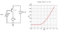
For a PMOS the source node is tied to VDD (Say 1.8). So at the gate you may connect a DC voltage source having a value VDD-VSG (parametrized) i.e 1.8-VSG. Now do a DC sweep for the VSG parameter from 1.8 to 0 and plot Ids. This should give you Ids Vs Vsg plot. Yo may do similar thing with the drain node to get Ids Vs VSD plot.

In Cadence ADE look for DC sweep and Parametric analysis ... I dont remember which one will work but you can try with both of them..

Hope this will help... :)
 

Hi Hazra, thanks for the input.

Taking into account what you said and after studying a little the material on PMOS transistors, I think I got it. The examples that I saw were with the source attached to the ground, a battery with the negative terminal to the gate and the positive one to the ground and another battery with the negative terminal to the drain and positive to ground. Maybe it was this that confused me.

From what I could understood, whatever the voltage at the source, the gate voltage must be bellow the source.

For example, in the NMOS we start from 0 up to Vdd, in my case, I did a parametric with VG= 0V, 1.2V, 2.1V and 3.3V.

In this case, with the PMOS, I can do something like:

- Source from PMOS connected to VDD = 3.3V, Drain to GROUND, GATE with a VDC (with the + signal attached to the GATE and the - signal to ground).

- Then, starting with VG = +3.3 -> VSG = VS - VG = 3.3 - 3.3 = 0V -> cut-off.

- VG = +2.1V -> VSG = VS - VG = 3.3 - 2.1 = 1.2V -> maybe triode;

- VG = 1.2V -> VSG = VS - VG = 3.3 - 1.2 = 2.1V -> maybe saturation;

- VG = 0V -> VSG = VS - VG = 3.3 - 0 = 3.3V -> maybe deep saturation;

I am right? Please feel free to correct me.

Kind regards and thanks in advance.

EDIT: I've forgotten to ask another thing. In case I want to use a IDC current source, I should connect it between the source and drain?
 
Last edited:

Hi AMSA,

Yes you are correct mostly. But I have confusion with the triode region (at VG = 2.1V) .... Your Drain is 0V so VSD = 3.3V and VSG=1.2V that means VSG - VTH << VSD so it should be in saturation.

The Ids Vs Vgs graph starts with cut-off, then sub-threshold, the saturation and then linear (if VSG -VTH > VSD) .... So in your case as VSD and VDS both can be max 3.3V so you should not get linear region.
Cadence reports a "region" variable, check that variable for the operating region of that MOSFET.

Again why dont you try VG = 3.3, 2.8 (Assuming Vth = 600mV so you will get to see the sub-threshold region), 2.1, 1.2 & 0 keeping VD at 1V (you will get to see linear as VG -> 0V)

And for IDC you can connect it at the drain terminal (as a sinking current source) for the PMOS. But using IDC you wont be able to plot Ids Vs Vgs because in this plot the Ids is the dependent variable and Vgs is the independent variable which we sweep.

Hop this will help ... :)
 

HI Hazra and thank you again for the reply.

Concerning the detail that you mentioned about "But I have confusion with the triode region (at VG = 2.1V) .... Your Drain is 0V so VSD = 3.3V and VSG=1.2V that means VSG - VTH << VSD so it should be in saturation." I just gave those voltages as an example. Doesn't mean that they accurately describing the behavior of the transistor. The sweep that I am doing is with a step of 0.33V.

Just a correction Hazra: VSG - VTH << VSD => VSD > VSG - VTH. When we have VSD > VSG - VTH (assuming a VTH=0,6V) means that the transistor is in saturation, right?

For saturation: Vsg > 0 & Vsd > Vsg - Vth;
For triodo: Vsg > 0 & 0 < Vsd < Vsg - Vth;
For cut off: Vsg < 0;

Despite this, the circuit that I used to trace the DC characteristics was the following: vdc attached between the source (+ of the vdc) and the gate (- of the vdc) and another vdc attached between the source (+ of the vdc) and drain (- of the vdc). Then I connected the source (and therefore the + of the vdc's) to ground.

To trace the Ids vs Vgs I am using what you have suggested, but instead of 1V I have used 50mV, 100mV and 150mV.
 

Hi AMSA,

Please check the picture attached and let me know your views .... you can also vary the VD to see different nature of the plot


Status
Not open for further replies.

Part and Inventory Search

Welcome to EDABoard.com

Sponsor

Back
Top