Continue to Site

Welcome to EDAboard.com

Welcome to our site! EDAboard.com is an international Electronics Discussion Forum focused on EDA software, circuits, schematics, books, theory, papers, asic, pld, 8051, DSP, Network, RF, Analog Design, PCB, Service Manuals... and a whole lot more! To participate you need to register. Registration is free. Click here to register now.

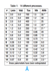
Can anyone provide me a sheet which describe at what tech-node which Vdd for MOS?

Status
Not open for further replies.

Rahul Sharma

Member level 3
Member level 3
Joined
Sep 9, 2014
Messages
63
Helped
4
Reputation
8
Reaction score
4
Trophy points
8
Location
Guwahati, INDIA
Activity points
506
as TSMC/UMC 130nm we can use 1.2/3.3V. Kindly provide me any link explaining Technology vs power-supply for MOS technology.
 

There are references and manual from manufacturers of MOS chip. Check website and Google search.
 

... Technology vs power-supply for MOS technology.

Here are 2 tables with different processes/voltages. Forgot where I found them.
14_different_processes.png process-parameters_vs_process-sizes.png

Note: the stated VDD voltages are core voltages. Higher I/O voltages may be used with optional thick oxide.
 
Here are 2 tables with different processes/voltages. Forgot where I found them.
View attachment 129694 View attachment 129695

Note: the stated VDD voltages are core voltages. Higher I/O voltages may be used with optional thick oxide.

What about below technologies such as 28nm and 14nm. What is power supply and vth for these lower feature size.
 

Status
Not open for further replies.

Part and Inventory Search

Welcome to EDABoard.com

Sponsor

Back
Top