Continue to Site

Welcome to EDAboard.com

Welcome to our site! EDAboard.com is an international Electronics Discussion Forum focused on EDA software, circuits, schematics, books, theory, papers, asic, pld, 8051, DSP, Network, RF, Analog Design, PCB, Service Manuals... and a whole lot more! To participate you need to register. Registration is free. Click here to register now.

Calculate the resistance of metal layer

Status
Not open for further replies.

tok47

Advanced Member level 4
Full Member level 1
Joined
Jan 16, 2004
Messages
119
Helped
0
Reputation
0
Reaction score
0
Trophy points
1,296
Location
Kuala Lumpur, MALAYSIA
Visit site
Activity points
1,013
Hi ALL,

I had a metal layer of bus signal which i wish to calculate the effective resistance of this layer.

Please see the attachment file for the layout.

Can i just calculate the whole rectangle and minus the the empty space to get the effective resistance? will it be accurate?

Thanks.

Rdgs
YY

p/s : {[(X * Y) - (area of the empty space)] * sheet resistance }= effective resistance
 

Attachments

  • layou_sample.png
    layou_sample.png
    22.3 KB · Views: 463

Can i just calculate the whole rectangle and minus the the empty space to get the effective resistance? will it be accurate?

{[(X * Y) - (area of the empty space)] * sheet resistance }= effective resistance

No: [(Y/X) - (Y/X of all empty space areas)] * sheet resistance }= effective resistance
 

As far as I've correctly understood your question, I don't agree neither with you formula nor with the formula of erikl.

The DC resistance of a metal sheet is given by R=ρ*L/A where ρ is the resistivity, L the lenght along with the current flows and A is the cross-section. Is the sheet has thickness T, and width W then A=W*T from which: R=ρ*L/(W*T).
Now we can define the sheet resistance as Rs=ρ/T so that the total resistance can be written as: R=Rs*L/W.

Then a first problem is to know if in your case the current will flows along X or Y. If it flows along Y, then R=Rs*Y/X otherwise R=Rs*X/Y.
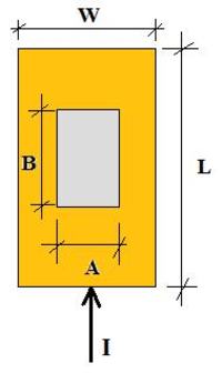
Let's consider now a rectangular hole of dimensions AxB with A parallel to W and B parallel to L as in this drawing:


In this case we have that for a length L1=L-B, the width is W1=W
while for a length L2=B the width is W2=W-A

then the total resistance (valid only if the current is flowing along L) will be;

R=Rs*(L1/W1+L2/W2)=Rs*[(L-B)/W+B/(W-A)]

after some simple manipulation:

R=Rs*[L/W+A*B/(W*(W-A)]

thus the total resistance:

1) depends from the path of the current
2) increases removing metal
3) depends from the shape of the holes.
 
Last edited:
then the total resistance (valid only if the current is flowing along L) will be;

R=Rs*(L1/W1+L2/W2)=Rs*[(L-B)/W+B/(W-A)]

This is a good zero-order model / formula.

In fact, in structures with holes (slots) the current flow is never uni-directional - the current will flow around the holes, creating 2D patterns of current flow.

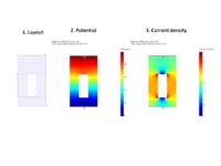
I did a quick simulation of a similar structure - here is the layout and simulation results (potential and current density plots).


Resistance calculated by the formula (sheet resistance of the metal was set to 50 mOhm/sq) is 0.1125 Ohm (there are 2.25 effective squares), while numerical simulation gives a resistance of 0.1179 Ohm. The difference is ~5%, not much (for most purposes) - but can be higher, depending on the layout.

In fact, the layout shown in the original post looks like a part of power net or power transistor. Resistance is only one part of the problem, the other one is current density (electromigration).

To minimize current density, one should avoid placing slots on the path of high current density, avoid having large current going around a sharp (e.g. 90 degree) corner, etc. etc.

Performing a mesh-based simulation (like the one shown above) helps to understand how the current flows, and to optimize the layout to minimize current density and resistance.

Sometimes, you should not minimize the resistance, but to route the current in a balanced (i.e. uniformly distributed) manner - by providing current ballasting mechanisms (meaning - adding some resistance somewhere).

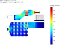
Here is an example of simulation of a more complex structure (tapering metals, metal mesh, many metal layers, via arrays, etc. etc.):

 
To minimize current density, one should avoid placing slots on the path of high current density, avoid having large current going around a sharp (e.g. 90 degree) corner, etc. etc.

Thanks to litho dispersion - even with phase masking - we never achieve such sharp corners on silicon. And if we had them, nevertheless, say in a 1µm process - wouldn't electromigration round them after some time - really high current densities assumed?
 

Thanks to litho dispersion - even with phase masking - we never achieve such sharp corners on silicon.

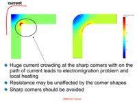
Yes and no. Of course, lithography and resist etching will lead to some corner rounding - bit clearly not enough to reduce current crowding in wide metal traces (say 50 um and larger) used in power nest and in power devices. The radius of curvature due to litho/etch is much smaller than the metal trace width (for high currents), and radius of curvature should be comparable with the trace width, to avoid current crowding. Please have a look at this illustration:


And if we had them, nevertheless, say in a 1µm process -
wouldn't electromigration round them after some time - really high current densities assumed?

Not necessarily - if you create a perfect layout, from current routing / ballasting viewpoint - there will be no burnout due to electromigration in the first place.
With electromigration burnout - this process may or may not stop. Imagine a row of contacts/vias with non-uniform current distribution (current is highest in the edge via) - the edge via will burn our first, then the next, and so on.

Further, other problems may kick in, due to high current crowding - such as localized heating, pulsed in time (DC-DC converter), leading to thermal mismatch and mechanical stress, leading to cracking of passivation, leading to corrosion and chip reliability issue - I am describing a real case seen in real life...
 
This was a great thread for me trying to understand how R is computed for some simple geometry. Thanks especially to timof for his diagrams that made it all "click".

What software can be used to compute those current diagrams and precise R values? I suspect there are several tools, but whenever I search for R solvers it talks about things like StarRC which isn't an exact (finite element) solution, just good heuristic in order to be fast.
 

Status
Not open for further replies.

Part and Inventory Search

Welcome to EDABoard.com

Sponsor

Back
Top