Continue to Site

Welcome to EDAboard.com

Welcome to our site! EDAboard.com is an international Electronics Discussion Forum focused on EDA software, circuits, schematics, books, theory, papers, asic, pld, 8051, DSP, Network, RF, Analog Design, PCB, Service Manuals... and a whole lot more! To participate you need to register. Registration is free. Click here to register now.

Buck converter ----- why the LCR part influence the input voltag of the switch driver

Status
Not open for further replies.

nelly1

Junior Member level 3
Joined
Jun 14, 2012
Messages
29
Helped
0
Reputation
0
Reaction score
0
Trophy points
1,281
Visit site
Activity points
1,495
problems about synchronous Buck converter with 2 switch

For my DCDC BUCK CONVERTER:
Vin=3.6V Vout=1.2V Iout=150mV f=1MHZ L=8uH C=0.25uF R=8Ω Vin1 signal=0-1.2V Vin2 signal=(2.4-3.6V)

I'm using the schematic below as the synchronous switch part for my buck converter.When Vin1 from 0-1.2, Vin2 from 2.4-3.6, nmos switch stack become "on" and pmos switch stack become "off" . Vout from 3.6-0 and vice versa.
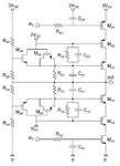
bild1.jpg
It works quite well with a 100f capacitor as load and can provide me a pulse signal from 0-3.6V. The problem is, when i added these part into the buck converter system, the Vin1 signal (0-1.2V) after the RC lowpass looks like the picture 2,which belows 0 and then turn the Mn1,2,3 switch on(which i don't what it to happen.....)

bild2.png

My output now is something below.
bild3.png
I think the problem comes because the pmos switch is open and the nmos swtich also is open,so the current in inductor has no place to flow.
can I just add a diode in parallel with my nmos switch??????
 
Last edited:

Re: problems about synchronous Buck converter with 2 switch

I think the problem comes because the pmos switch is open and the nmos swtich also is open,so the current in inductor has no place to flow.

Looking at this particular issue...

Yes, if the coil suddenly sees high impedance, it will overcome it with a high voltage spike (or arcing), as the flux field collapses.

Your waveforms have a couple of spikes, but they do not look too severe.

can I just add a diode in parallel with my nmos switch??????

In a buck converter the low side switch (assuming that is where you have an N-mosfet) needs to be able to carry current upward.

The question becomes whether to let the body diode do the job, or whether to install the N-mos upside-down, or whether to use P-mosfets to do both switch roles. Etc.
 

Re: problems about synchronous Buck converter with 2 switch

thanks a lot!
And i have another question about the dead-time control for the synchronous buck.
When i use switch stack like the schematic shows in bild1,can i just consider the dead time control to be something like : i only need to make the first Mp1 closed(MP2,MP3 still open) and then make the Mn1 open(Mn2, Mn3 still closed)? or i should make first all 3 high side pswitches closed, then allow the low side to be opened?
 

I am running a simulation of your schematic.

1.

From what I can see, all of the M2 & M3 switches are always biased ON. However they do not conduct when their respective M1 switch is biased OFF.

2.

And i have another question about the dead-time control for the synchronous buck.

My simulation probably needs adjusting, but the waveform I see at the output has its transitions 'softened' by the action of all those capacitors. This may permit the high side to turn on as the low side is turning off (and vice-versa). Perhaps that is better than creating any 'dead time' while the coil is energized.

The reason is that the coil will want to send its energy somewhere. If it sees high impedance even for a microsecond, then your inductive time constant (L / R) becomes 8uH divided by a very high number. In one microsecond your coil could deliver a very high voltage spike.

However there is a kind of 'dead time' which might be okay. It would be the idle time when the coil has discharged completely, when running in discontinuous mode. For the remainder of the cycle the low side is On, the high side is Off.

3.

Remember that current will need to flow upward from ground, and through the low side totem pole (Mn1-Mn2-Mn3).

While you are in the development stage, for the time being it may be easier simply to install a diode pointing upward.

4.

I am not sure about the purpose for such a complicated driver network. Was this presented as the proper synchronous driver to use?

5.

I believe this network is connected to your buck converter somehow. It would help if you were to post the complete schematic.
 

1. you are right. And the both side influence each other. like When VdMn1 starts to go higher, then the Vout goes higher and meanwhile the VdMp1 goes higher.

2. Actually i don't want my buck converter to work at DCM because of the efficiency. Till now, when the Vout change from 0-3Vdd , I can't turn off all the low side switch before opening the high side.(as i mentioned in point 1, the influence each other). The only thing i m not sure is about the switch overlapping.I just wonder if i turn off the Mn1(but Mn2,Mn3 still on), and then turn on the Mp1, is that acceptable?

3.I plan to use the Psub to Dnwell diode as the diode pointing upward.

4. I want to use this one as the synchronous driver......(or accurately as the dynamic biasing+power stage)

5. the schematic is shown as below. the PNmos_ps_driver is the same like Bild1.
**broken link removed**
 

There is a lot going on in this circuit, and I find it is still too much to get my mind around.

You might be better able to decide whether it suits your needs if you watch it operating in an animated simulator.

Below is the link to my simulation of your schematic using the software at falstad.com/circuit.

Clicking it will open the website, load the schematic, and run it on your computer. (Click Allow to load the Java applet.) You can see the direction and intensity of current flow at every moment in the cycle.

https://tinyurl.com/bv83mhy

I had to run it at a higher voltage than your original spec.

You may have to maximize the window size so it fits the entire display.
 

yes...it's really a lot.. thank you very very much!:)
 

Status
Not open for further replies.

Part and Inventory Search

Welcome to EDABoard.com

Sponsor

Back
Top