Continue to Site

Welcome to EDAboard.com

Welcome to our site! EDAboard.com is an international Electronics Discussion Forum focused on EDA software, circuits, schematics, books, theory, papers, asic, pld, 8051, DSP, Network, RF, Analog Design, PCB, Service Manuals... and a whole lot more! To participate you need to register. Registration is free. Click here to register now.

Buck converter Error Amplifier Circuit Parameters, need an urgent help

Status
Not open for further replies.

Mustafatarhan49

Junior Member level 2
Joined
Aug 20, 2012
Messages
20
Helped
1
Reputation
2
Reaction score
1
Trophy points
1,283
Activity points
1,430
Hello guys,

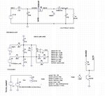
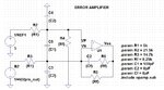
I wanna know how the designer calculated the below error amplifier circuit component values in the attached figure. Can anyone help me to figure out how to calculate this compensation values?
And I also wanna know which type of compensation network is this. I will appriciate if you can help me!
Thanks a lot!

Regards,
 

Attachments

  • forum.jpg
    forum.jpg
    164.7 KB · Views: 189

It's a very odd circuit, especially C1 which shouldn't have any impact on the circuit (except once the GBW of the op amp is exceeded).

I simulated its behavior and it doesn't appear to have a useful transfer function for an error amplifier. Low gain at low frequencies, no gain boost, prone to instability... are you sure that's the full schematic with the right values? I don't see R2 or R3 on the schematic.
 
[QUOTE ]It's a very odd circuit, especially C1 which shouldn't have any impact on the circuit (except once the GBW of the op amp is exceeded).

I simulated its behavior and it doesn't appear to have a useful transfer function for an error amplifier. Low gain at low frequencies, no gain boost, prone to instability... are you sure that's the full schematic with the right values? I don't see R2 or R3 on the schematic.[/QUOTE]

Actually, this is the circuit that I've used for the buck converter design compensation network. The complete circuit is in the attached file, please see. I actually, wantted to use type 3 compensation but i was getting to big flactuations in the output. Then I found this error amplifier circuit and aplpied it to my circuit and it was not good but at least i could see the output voltage in desired range. I have no clue about what to do :(

[QUOTE ] Without knowing what is being compensated, it's difficult to know what the circuit does. [/QUOTE]
I will compensate output voltage of the buck regulator. I have max 60V input, 6V output, 50mA load current 150kHz switching freq, 1.02mH inductor, 0.47uF output caps. And the circuit attached is used to compensate output voltage.

For your help thanks a lot in advance

- - - Updated - - -

=============================================================

attached figure just in the right side is the calculated compensation type 3 values for the circuit. The output is so odd here. That's why i used the first circuit, but i did not understand the circuit :) forum3.png
 

Attachments

  • forum2.jpg
    forum2.jpg
    207.5 KB · Views: 145

Are you just simulating results, or have you actually built the circuit?

For simulation, you should do a small signal average model of the buck converter, meaning you replace the switching components with an analog voltage which is proportional to the error amplifier output. That will allow you to look at things like stability and transient response, independent of the details of the switching action.

If you have LTspice files then go ahead and post them.

Yes, I am just simulating. I will not build the circuit.

- - - Updated - - -

Please see the attached .rar file, You can see the LTspice files. I will glad if you can show me how to do small signal average model.
Thanks in advance!
 

Attachments

  • buck converter results.rar
    3.5 KB · Views: 149

Why are the simulation results "not good"? Mine showed an initial output overshoot (which is normal due to the LC output resonance) and then settled to a steady-state 5V. To eliminate the overshoot you will need to add some sort of soft-start circuitry (Edit: Such as a slow start-up of the VREF1 voltage).

Here's a good tutorial on how to compensate switching regulators.
 
Last edited:

Why are the simulation results "not good"? Mine showed an initial output overshoot (which is normal due to the LC output resonance) and then settled to a steady-state 5V. To eliminate the overshoot you will need to add some sort of soft-start circuitry (Edit: Such as a slow start-up of the VREF1 voltage).

Here's a good tutorial on how to compensate switching regulators.

For the first circuit (which name is buck son dogru) output voltage is regulating between 10V and 24V. For the second circuit, as you said there is an overshoot in the begining then it is stable at 5V. First one is designed as a result of the compensation calculation for type3 network that i did. but it is not working properly (Please see the simulation). The second one, I have no clue how does the error amplifier components are calculated.
 

The error amplifier compensation components are calculated to cancel the effects of the LC output filter resonance. The ap note I referenced in my previous post will give you a clue. ;-)
 
Yes, I am just simulating. I will not build the circuit.

- - - Updated - - -

Please see the attached .rar file, You can see the LTspice files. I will glad if you can show me how to do small signal average model.
Thanks in advance!
Attached is a modification for small signal AC analysis. Now you can check stability margins, etc.
 

Attachments

  • buck ss.rar
    1.1 KB · Views: 108
Attached is a modification for small signal AC analysis. Now you can check stability margins, etc.

Man! that's too helpful! thank you thank you so much! One more question, How am i going to understand about the stability and transient response by looking to that results? I am really appriciated!


'crutschow', now I am reading the app note that you send, hopefully I will understand why the system is unstable.
Read these app notes for an explanation of stability margins.
https://www.venable.biz/tp-01.pdf
https://www.venable.biz/tp-03.pdf

Basically you look at the open loop response and try to achieve a desired crossover frequency (somewhere around a tenth of you switching frequency is a good start) and good phase margin (60 degrees is good). The transfer function of the error amplifier is adjusted to meet those requirements.

Thanks a lot! I will start to read now.
 

hi again,

after reading this ap notes, i made my compensation network, but eventhough i used same formulation and metholodology, my system looks unstable. why do you think that i can have unstability in the output in the system. In the attached file you can see the LTspice file. besides, i checked somewebsites for the soft start but it seems really hard to make it without an ic which has softstart future. Any idea how can i do this soft start in simulation?

Thanks a lot in advance!
 

Attachments

  • buck ss.rar
    2.6 KB · Views: 101

I have connected one big capacitor and resistor behind of Vref and it helped too much! :)

do you think if this consept can work on the pcb? what should i consider as a critical point here ? I will glad to here your advices?
 

I noticed a couple significant problems with your "Buck final.asc" design.

First, you do not have a PWM modulator circuit. For that you need to change V2 from a pulse source to a sawtooth. It's the relation of the error voltage to the sawtooth voltage that determines the pulse width generated at the output of U3. To change V2 to a sawtooth make Trise 99µs, Tfall 1µs and Ton 0.

The other thing is that your output filter capacitance is too small for the PWM switching frequency of 10kHz (1/100µs). 100µF for C1 allowed a stable simulation. That's not necessarily an optimum value and may affect the compensation values you have calculated, but it does give stable results.

I didn't check your compensation values, so don't know if they are optimum.

So how did you determine the value for the "big" capacitor? For a soft-start to minimize overshoot, use an RC time-constant (series R, capacitor to ground) of about 2ms at the Vref output.

What is the purpose of R2? :-? It's just an unnecessary load on V1.
 
I noticed a couple significant problems with your "Buck final.asc" design.

First, you do not have a PWM modulator circuit. For that you need to change V2 from a pulse source to a sawtooth. It's the relation of the error voltage to the sawtooth voltage that determines the pulse width generated at the output of U3. To change V2 to a sawtooth make Trise 99µs, Tfall 1µs and Ton 0.

Thanks for the nice explanation. Actually, you are right that i am not using pwm modulator and i should use sawtooth instead of pulse by changing Trise 6.5µs, Tfall 0.1µs and Ton 0. (150kHz switching freq)
The other thing is that your output filter capacitance is too small for the PWM switching frequency of 10kHz (1/100µs). 100µF for C1 allowed a stable simulation. That's not necessarily an optimum value and may affect the compensation values you have calculated, but it does give stable results.

I didn't check your compensation values, so don't know if they are optimum.

So how did you determine the value for the "big" capacitor? For a soft-start to minimize overshoot, use an RC time-constant (series R, capacitor to ground) of about 2ms at the Vref output.

What is the purpose of R2? :-? It's just an unnecessary load on V1.

Actually, my switching frequency is 150kHz and i have calculated capacitor value from the equation of C = Iripple /(8*Vripple*fswitch) = 35x10^-3 / (8*100*100^-3*150000) = 0.3uF

I have used R2 to turn on and off the gate. To turn a PMOS device OFF, Vgs must be ≈0V. I connect the source to +50V, so the gate voltage would have to swing from 50V when off to about 45V (with a logic level device) when ON.
 

hi again,

after reading this ap notes, i made my compensation network, but eventhough i used same formulation and metholodology, my system looks unstable. why do you think that i can have unstability in the output in the system. In the attached file you can see the LTspice file. besides, i checked somewebsites for the soft start but it seems really hard to make it without an ic which has softstart future. Any idea how can i do this soft start in simulation?

Thanks a lot in advance!
Your small signal compensation looks okay, I'm seeing a crossover frequency of about 80KHz with a phase margin of about 50 degrees. It should be stable (in the small signal sense).

Looking at the transient simulation, it looks like there are many problems with the PWM modulation. Like crutschow pointed out you don't have any ramp signal, which means things simple won't work. Also your switching frequency needs to be at least twice your crossover frequency, in practical terms a factor of five is more reasonable. Also I doubt your gate drive circuit will work effectively at 150KHz, it's probably too slow.
 
You're correct about R2 of course. I didn't look carefully at the schematic and thought it went to ground, not the MOSFET gate. :oops:

You don't seem to have enough output capacitance to give a reasonable low ripple voltage. I got a reasonably stable output by changing C1 to 20µF, reducing the loop gain by changing R5 to 42kΩ, and rolling off the loop response by changing C4 to 1nF (Those are not optimum values since there is still some low-level oscillation in the inductor current). The output ripple was about 20mVpp with those values.

I used a soft-start time-constant of 0.6ms, which avoids any significant start-up overshoot.

Note that you should have a resistor in series with Q1's collector since there's nothing to limit the current through the zener diode D2 when Q1 is ON. Something between 500Ω and 1kΩ should work.
 
Last edited:
Status
Not open for further replies.

Similar threads

Part and Inventory Search

Welcome to EDABoard.com

Sponsor

Back
Top