Continue to Site

Welcome to EDAboard.com

Welcome to our site! EDAboard.com is an international Electronics Discussion Forum focused on EDA software, circuits, schematics, books, theory, papers, asic, pld, 8051, DSP, Network, RF, Analog Design, PCB, Service Manuals... and a whole lot more! To participate you need to register. Registration is free. Click here to register now.

Buck boost converter not working

Status
Not open for further replies.

Phrancees69

Newbie level 6
Newbie level 6
Joined
Feb 16, 2022
Messages
12
Helped
0
Reputation
0
Reaction score
0
Trophy points
1
Activity points
117
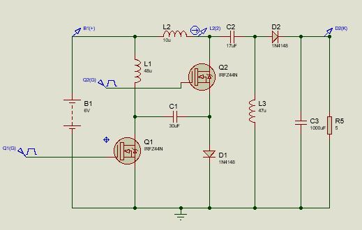
Hi engineers, I need help with my buck boost converter. I designed a high gain buck boost converter and it works perfectly on simulation (Proteus/Ltspice). However when I build the prototype on pcb and breadboard it doesn't work. My circuit has two switches; high and low side. I have tried ir2110 and hcpl3150 optocoupler switch drivers and the the drivers work just fine as they supply the required gate pwm pulses. but the main converter is not working. I also notice that whenever I turn on the power supply, the value drops drastically and there is no output from my converter. My circuit schematic is posted, kindly check to discover errors. Thank you
bbcnv.JPG
 

Hi,

the value drops drastically
Which value?

but the main converter is not working
"Is not working" is no error description. You need to tell your test conditions, what you expect and what you see instead.

All in all you give information about "it works". You show the "working" schematic.
But you don´t show us information of the "not working circuit".
(it´s like your bike is broken, but you give your brother´s good bike to the garage).

So all we can do is: guess.
* gate drive signals are wrong: We neither see the gate drive circuit, nor the voltage levels, nor the timing...
* Your PCB/wiring is wrong: I´d generally say a breadboard is not suitable for switching power applications. In best case a breadboard circuit does "something", but usually not with the expected performance. I expect ringing, oversoot, instability.. but it´s very likely it does nothing.
* your MOSFET are already killed by overvoltage. I expect high voltage, I expect spikes, but I don´t see any protection.
* other parts (like 1N4148) are killed. (you surely know that an 1N4148 is specified for 150mA (average rectified current @ good heat spreading)
* your circuit differs from the given schemaitc. Regarding wiring and/or part values. I guess you don´t really have a 17uF and and a 30uF capacitor ... and I guess you don´t use non polarized as in your

My recommendation for the non working circuit:
* focus on the malfunction
* take a sheet of paper and a pencil and draw down "what you expect". Do this for each node from signal input to output.
* after the drawings .. do the measurements and compare them with your expectations (drawings).
* on mismatch: find out whether your expectation was wrong or the circuit is wrong.

***
But you said you did a simulation. So you can see the timing, magnitude and waveform of every node.
This is the main benefit of a simulation. It (falsly) shows a working circuit, where a real circuit immediately gets killed by overvoltage or overcurrent. So use this feature to find out whether each of your used devices is operation within specification.

Klaus
 
thank you very much Klaus for your lucid explanation. Sorry for not providing complete details of my circuit. My circuit is summarily a reconfigured combination of Cuk and SEPIC converters operating at 50kHz. It is supposed to boost a 6V input to 14V output under a duty cycle of 60% and buck an 18V input to a 14V output under a duty cycle of 20%.
For the discrete components in the prototype, I am using 22uF and 33uF capacitors to replace the 17uF and 33uF capacitors respectively. I have tried them in simulation and they worked just fine. The driver circuit (tried HCPL3150 & IR2110) is driven by Arduino. I am not sure i have problems with the driver circuit. My main concern is the diminished input voltage of the converter (as seen on the dc power supply). Also, from your comments you mentioned overvoltage and spikes on the MOSFET, any idea on how i can detect these?
I will review the circuit again using the suggestions you provided. I have also attached the photo of the test pcb for your viewing. I connected two 10ohms resistor in parallel to obtain a 5 ohms load resistance.

Thank you
pcb2.jpeg


pcb1.jpeg
 

I'm not sure how the circuit is supposed to work in general, posting the LTspice simulation circuit might help to understand it.

I'm however pretty sure that Q2 can't be driven by IR2110, because source voltage swings below GND. You didn't post the driver circuit, so we don't know how you connected it exactly.
 
show the control please photo's and schematics ...

it does appear from the power hardware picture - that there is really very little chance of this university project ever working ...


"my car won't start - just the battery voltage falls when I turn the key " - " what is wrong with my car ? "

see the similarity to your post .... ?
--- Updated ---

what is the current limit of your power supply ?
--- Updated ---

1N5822 is only 40V rated, spikes can easily kill these - have you used your sim to see the voltages on the semis ?
 
Hi,


Which value?


"Is not working" is no error description. You need to tell your test conditions, what you expect and what you see instead.

All in all you give information about "it works". You show the "working" schematic.
But you don´t show us information of the "not working circuit".
(it´s like your bike is broken, but you give your brother´s good bike to the garage).

So all we can do is: guess.
* gate drive signals are wrong: We neither see the gate drive circuit, nor the voltage levels, nor the timing...
* Your PCB/wiring is wrong: I´d generally say a breadboard is not suitable for switching power applications. In best case a breadboard circuit does "something", but usually not with the expected performance. I expect ringing, oversoot, instability.. but it´s very likely it does nothing.
* your MOSFET are already killed by overvoltage. I expect high voltage, I expect spikes, but I don´t see any protection.
* other parts (like 1N4148) are killed. (you surely know that an 1N4148 is specified for 150mA (average rectified current @ good heat spreading)
* your circuit differs from the given schemaitc. Regarding wiring and/or part values. I guess you don´t really have a 17uF and and a 30uF capacitor ... and I guess you don´t use non polarized as in your

My recommendation for the non working circuit:
* focus on the malfunction
* take a sheet of paper and a pencil and draw down "what you expect". Do this for each node from signal input to output.
* after the drawings .. do the measurements and compare them with your expectations (drawings).
* on mismatch: find out whether your expectation was wrong or the circuit is wrong.

***
But you said you did a simulation. So you can see the timing, magnitude and waveform of every node.
This is the main benefit of a simulation. It (falsly) shows a working circuit, where a real circuit immediately gets killed by overvoltage or overcurrent. So use this feature to find out whether each of your used devices is operation within specification.

Klaus
I meant to
Hi,


Which value?


"Is not working" is no error description. You need to tell your test conditions, what you expect and what you see instead.

All in all you give information about "it works". You show the "working" schematic.
But you don´t show us information of the "not working circuit".
(it´s like your bike is broken, but you give your brother´s good bike to the garage).

So all we can do is: guess.
* gate drive signals are wrong: We neither see the gate drive circuit, nor the voltage levels, nor the timing...
* Your PCB/wiring is wrong: I´d generally say a breadboard is not suitable for switching power applications. In best case a breadboard circuit does "something", but usually not with the expected performance. I expect ringing, oversoot, instability.. but it´s very likely it does nothing.
* your MOSFET are already killed by overvoltage. I expect high voltage, I expect spikes, but I don´t see any protection.
* other parts (like 1N4148) are killed. (you surely know that an 1N4148 is specified for 150mA (average rectified current @ good heat spreading)
* your circuit differs from the given schemaitc. Regarding wiring and/or part values. I guess you don´t really have a 17uF and and a 30uF capacitor ... and I guess you don´t use non polarized as in your

My recommendation for the non working circuit:
* focus on the malfunction
* take a sheet of paper and a pencil and draw down "what you expect". Do this for each node from signal input to output.
* after the drawings .. do the measurements and compare them with your expectations (drawings).
* on mismatch: find out whether your expectation was wrong or the circuit is wrong.

***
But you said you did a simulation. So you can see the timing, magnitude and waveform of every node.
This is the main benefit of a simulation. It (falsly) shows a working circuit, where a real circuit immediately gets killed by overvoltage or overcurrent. So use this feature to find out whether each of your used devices is operation within specification.

Klaus
Hi, I meant to say the DC voltage value from the supply. For example, if I supplied my circuit with an input voltage of 6V, as soon as i energize the circuit, the input voltage on the meter reduces to about 0.6 volts. Hence, there is no energy flowing in my circuit.
 

show the control please photo's and schematics ...

it does appear from the power hardware picture - that there is really very little chance of this university project ever working ...


"my car won't start - just the battery voltage falls when I turn the key " - " what is wrong with my car ? "

see the similarity to your post .... ?
--- Updated ---

what is the current limit of your power supply ?
--- Updated ---

1N5822 is only 40V rated, spikes can easily kill these - have you used your sim to see the voltages on the semis ?
Thank you for your reply.
Here is the schematic on ltspice. I couldn't find 1N5822 diode on ltspice library
1664278936339.png

I'm not sure how the circuit is supposed to work in general, posting the LTspice simulation circuit might help to understand it.

I'm however pretty sure that Q2 can't be driven by IR2110, because source voltage swings below GND. You didn't post the driver circuit, so we don't know how you connected it exactly.
 

show the control please photo's and schematics ...

it does appear from the power hardware picture - that there is really very little chance of this university project ever working ...


"my car won't start - just the battery voltage falls when I turn the key " - " what is wrong with my car ? "

see the similarity to your post .... ?
--- Updated ---

what is the current limit of your power supply ?
--- Updated ---

1N5822 is only 40V rated, spikes can easily kill these - have you used your sim to see the voltages on the semis ?
Thank you for your response. I posted the circuit already. These are the currents and voltages inductors and output resistor.
Also i just discovered that the voltage across most of the components is almost 40V, whereas my capacitors for example are rated just 25V. I need your advice on the circuit please. Thank you once again
1664279542630.png


1664279626562.png

1664279935047.png
 

Output calculates as 42 Watts. To get that from a 6V supply requires 7A average. I'm running a simulation of a basic boost converter. It shows that waveforms of 14 Amperes peak must go to the output stage (since it must happen during Off-time). It's the same amount of Amperes through your inductor, and drawn from your 6V supply.

Cuk and Sepic topologies have additional indicators and capacitors. They must carry that amount.

Parasitic resistance needs to be minuscule if it's going to work. A mere 1/10 of an ohm subtracts 0.6V from your effective supply voltage. I had to extend duty cycle to 75% in my simulation.

boost converter clk-driven 6v to 14v 3A 50kHz.png
 
LTspice schematic confirms my doubt that IR2110 high side driver is operated beyond its working voltage range. The limitation might not appear in used simulation model.

I'd prefer a .zip archive of LTspice files, including any non-standard library files.
But the provided simulation circuit clarifies at least intended circuit operation.

Generally I wonder if you expect any advantage over a basic SEPIC converter justifying the higher component count.
 
you pretty much have the whole story right here ...

"IR2110 high side driver is operated beyond its working voltage range." from FvM above
 

Hi,


Which value?


"Is not working" is no error description. You need to tell your test conditions, what you expect and what you see instead.

All in all you give information about "it works". You show the "working" schematic.
But you don´t show us information of the "not working circuit".
(it´s like your bike is broken, but you give your brother´s good bike to the garage).

So all we can do is: guess.
* gate drive signals are wrong: We neither see the gate drive circuit, nor the voltage levels, nor the timing...
* Your PCB/wiring is wrong: I´d generally say a breadboard is not suitable for switching power applications. In best case a breadboard circuit does "something", but usually not with the expected performance. I expect ringing, oversoot, instability.. but it´s very likely it does nothing.
* your MOSFET are already killed by overvoltage. I expect high voltage, I expect spikes, but I don´t see any protection.
* other parts (like 1N4148) are killed. (you surely know that an 1N4148 is specified for 150mA (average rectified current @ good heat spreading)
* your circuit differs from the given schemaitc. Regarding wiring and/or part values. I guess you don´t really have a 17uF and and a 30uF capacitor ... and I guess you don´t use non polarized as in your

My recommendation for the non working circuit:
* focus on the malfunction
* take a sheet of paper and a pencil and draw down "what you expect". Do this for each node from signal input to output.
* after the drawings .. do the measurements and compare them with your expectations (drawings).
* on mismatch: find out whether your expectation was wrong or the circuit is wrong.

***
But you said you did a simulation. So you can see the timing, magnitude and waveform of every node.
This is the main benefit of a simulation. It (falsly) shows a working circuit, where a real circuit immediately gets killed by overvoltage or overcurrent. So use this feature to find out whether each of your used devices is operation within specification.

Klaus
Output calculates as 42 Watts. To get that from a 6V supply requires 7A average. I'm running a simulation of a basic boost converter. It shows that waveforms of 14 Amperes peak must go to the output stage (since it must happen during Off-time). It's the same amount of Amperes through your inductor, and drawn from your 6V supply.

Cuk and Sepic topologies have additional indicators and capacitors. They must carry that amount.

Parasitic resistance needs to be minuscule if it's going to work. A mere 1/10 of an ohm subtracts 0.6V from your effective supply voltage. I had to extend duty cycle to 75% in my simulation.

View attachment 178742
Please what's the name of the simulator used in this illustration?
 

LTspice schematic confirms my doubt that IR2110 high side driver is operated beyond its working voltage range. The limitation might not appear in used simulation model.

I'd prefer a .zip archive of LTspice files, including any non-standard library files.
But the provided simulation circuit clarifies at least intended circuit operation.

Generally I wonder if you expect any advantage over a basic SEPIC converter justifying the higher component count.
Thank you for your response. I'm a newbie in circuits design. I also need to come up with some novelty in my design, hence I'm trying something different from the conventional SEPIC converter.
 

Please what's the name of the simulator used in this illustration?

Falstad's animated interactive simulator. Free to use and download at:

falstad.com/circuit

Also are you saying I increase my input current so as to achieve my desired output?

Parasitic resistance causes unwanted voltage drops. You must minimize such resistance in the current path, so that you obtain entire required current through your system.

I put 0.2 ohms in my simulation as an attempt to make it realistic. It robs several Watts of power. It forced me to lengthen duty cycle (switch On-time).

At low voltage a boost converter can only give you a limited amount of boost.
You may find it necessary to interleave two boost converters in order to achieve your desired output.

----------------------------------------------------

Side note: Connect load before you apply power to a boost converter. Otherwise output voltage soars into the high voltage range, with risk of destroying components.
 
Status
Not open for further replies.

Similar threads

Part and Inventory Search

Welcome to EDABoard.com

Sponsor

Back
Top