Continue to Site

Welcome to EDAboard.com

Welcome to our site! EDAboard.com is an international Electronics Discussion Forum focused on EDA software, circuits, schematics, books, theory, papers, asic, pld, 8051, DSP, Network, RF, Analog Design, PCB, Service Manuals... and a whole lot more! To participate you need to register. Registration is free. Click here to register now.

Bitwidth Management in Input and Output

Status
Not open for further replies.

beginner_EDA

Full Member level 4
Full Member level 4
Joined
Aug 14, 2013
Messages
191
Helped
0
Reputation
0
Reaction score
0
Trophy points
1,296
Visit site
Activity points
3,854
Hi,
I have two components:
1. Input: 1st component with 10 bit ADC and running at 100 MHz
2. output: 2nd component with Ethernet having 32 bit Avalon sink and also running at 100 MHz.

My aim is to connect both components and achieve full load/speed by using all 32 bit width of Ethernet. But the input is not only 10 bit and also running at same speed(100 MHz).

How I can map 10 bit input -> 32 bit output and at the same time maintaining full speed of Ethernet?

Here I read there is a possibility of using FIFO with different bit width but only multiple of 2.
https://www.altera.com/literature/ug/ug_fifo.pdf

Any idea will be highly appreciated?

Regards
 

Then I am just wasting 32-10=22 bit width of full speed/load of Ethernet. In other word, It will be just increasing redundancy.
Any other suggestions, please.
 

Then I am just wasting 32-10=22 bit width of full speed/load of Ethernet. In other word, It will be just increasing redundancy.
Any other suggestions, please.
Collect two or three inputs then write them to a 32 bit wide fifo. Fill the unused input data bits with 0.

Kevin Jennings
 

My aim is to connect both components and achieve full load/speed by using all 32 bit width of Ethernet. But the input is not only 10 bit and also running at same speed(100 MHz).
How I can map 10 bit input -> 32 bit output and at the same time maintaining full speed of Ethernet?
I don't really know what you mean by full speed of Ethernet...see below. I'll assume you are using GigE.

just pad the unused bits with 0s?
This will require more Ethernet bandwidth than the "full speed of Ethernet", 10 * 100 = 1000 Mbps (i.e. 1Gbps). If you are talking about a GigE connection then you'll already have a payload that exceeds the payload of Ethernet frames. You can get something like ~990Mbps sustained. If you're using a 10Gig Ethernet, then you won't be using anything close to the "full speed of Ethernet".

Then I am just wasting 32-10=22 bit width of full speed/load of Ethernet. In other word, It will be just increasing redundancy.
Any other suggestions, please.
Redundancy!? That makes no sense at all. 0 padding doesn't create any kind of redundancy.

Collect two or three inputs then write them to a 32 bit wide fifo. Fill the unused input data bits with 0.
Oh, boy more 0 fill redundancy ;-).
Oops K-J you're not using the "full speed of Ethernet". The OP obviously wants to send 1000 Mbps of ADC data, which doesn't use the "full speed of Ethernet"


beginner_EDA, Your problem definition is poorly written.

- - - Updated - - -

Maybe you want to find the optimal balance between Ethernet packet size and transmission latency?

If that is the case the most efficient in terms of transmission is to pick a packet size with a payload that is a multiple of 10-bits and 8-bits (so the payload is a integral number of bytes) and stuff the 32-bit input with 3 10-bit words + 2 bits of the 4th word, followed by 8-bits of the 4th word + 2 words + 4-bits of the 7th word...etc.

So the ADC data will be packed with no zero fill, and the packet size will be set to the smallest size that doesn't result in exceeding the total bandwidth of the connection (including the overhead). Doing something like this will reduce you're latency for the ADC data to the minimum sustainable value.
Hi thanks for idea. I am trying to implement it in Verilog/VHDL.

Could you please give some idea for mapping:
Source (Input) have following signal for 10 bit ADC:
Code:
 // source interface
input        System_Clock,
input        System_Reset,
input  [9:0]  ADC_data,
output      ADC_Clock

Sink (Output) have Avalon Streaming Sink Interface of 32 bit having following signals:
Code:
    // sink interface
    input           System_Clock,
    input           System_Reset,
    input           asi_snk0_valid,
    output          asi_snk0_ready,
    input   [31:0]  asi_snk0_data,
    input   [1:0]   asi_snk0_empty,
    input           asi_snk0_startofpacket,
    input           asi_snk0_endofpacket

How to map other signals apart from data one? and sorry if answer is so obvious.

regards
 

Hi thanks for idea. I am trying to implement it in Verilog/VHDL.

Could you please give some idea for mapping:
Source (Input) have following signal for 10 bit ADC:
// source interface
input System_Clock,
input System_Reset,
input [9:0] ADC_data,
output ADC_Clock
So you are driving the ADC_Clock from the FPGA and deriving it from the System_Clock? You do know that FPGAs are not that great for outputting a jitter free clock, therefore you're giving the ADC a jittery clock, which isn't great for getting good ADC output data samples.

Now about the mapping...I'm assuming you're intention wasn't asking someone to write the "mapping" of the ADC interface to the Avalon streaming sink.

The simplest solution is to just collect 3 ADC samples and stuff them into a single 32-bit word.
assign adc_word = {2'b00, sample[2], sample[1], sample[0]}
You will end up with 2-bits of zero padding, but the simplicity of the logic makes up for wasting some bandwidth. If you are set on utilizing the maximum bandwidth of the Avalon streaming interface then you'll need to reroute the samples into different positions.
adc_word = {sample[3][1:0], sample[2], sample[1], sample[0]}
next word...
adc_word = {sample[6][3:0], sample[5], sample[4], sample[3][9:2]}
(note: my indices are only to show you how the incoming samples get shifted around, so don't think this is usable code)
 
Now about the mapping...I'm assuming you're intention wasn't asking someone to write the "mapping" of the ADC interface to the Avalon streaming sink.
Hi,
This is what I wanted to ask. just some hints will be OK.
 

Hmm, 100Mhz, 10bit. This is 1000 Mbps exactly. Are you sure your ethernet connection will have no overhead at all? normally there are packet headers for ethernet/IP/UDP. You should check the documentation for the avalon ethernet, my guess is that start/end of packet are used to determine when to add the preamble and fcs.
 

Wow, you must not read past posts in a thread or you just like to "hear" yourself speak. I already brought that little tidbit up back in post #5.
 

Wow, you must not read past posts in a thread or you just like to "hear" yourself speak. I already brought that little tidbit up back in post #5.
Hi,
I have no comment about your support for my post. It always helped me to understand the concept and its implementation better. I accepted my mistake not looking throughly on the past post before posting this question and not gonna to be repeat. I am sorry. Now I look If I found some clue I am looking for on past posts.

I was referring to vGoodtimes, restating what I posted in #5 about the 10-bit at 100 MHz being 1000 MHz, i.e. 1Gbps. Their post has no added value to this thread (nor does this one, but it does clarify who the post was directed at)

Sorry about making it seem like I was telling you to read my post. :oops: My mistake for not using reply with quote.
 

Wow, you must not read past posts in a thread or you just like to "hear" yourself speak. I already brought that little tidbit up back in post #5.

Ah, good catch. I was in a bit of a rush when I posted this. I didn't have enough time to finish explaining what to look for in order to connect up the non-data signals in the interface.


@beginner_EDA
Can you describe the ethernet system in more detail? You will almost certainly need to determine how things like the UDP/IP/ethernet headers get added. Usually, you have to do most of the ethernet frame header and all of the UDP/IP header. The avalon interface itself is described on page 39 of https://www.altera.com/en_US/pdfs/literature/manual/mnl_avalon_spec.pdf . The ethernet system itself should describe what start/end of packet mean in the context of the start/end of an actual ethernet frame.

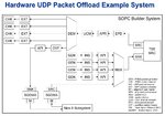
Hi, this is the implementation of Nios II UDP Offload Example

UDP.jpg
**broken link removed**

whose block diagram is in attachment.
As shown in block digram, GEN component generates the predefined payload and pass to INS component where all Ethernet, IP, UDP, etc. Header is added. API component add 2 byte for NIOS compatibility and then after muxing, data send to PC via TSE MAC. Its working as I observed the known sent data from GEN component in wireshark in PC.

All the source and sink interfaces between components follow this pattern:
Code:
input Clock,
input Reset,
input asi_snk0_valid,
output asi_snk0_ready,
input [31:0] asi_snk0_data,
input [1:0] asi_snk0_empty,
input asi_snk0_startofpacket,
input asi_snk0_endofpacket

and my aim is to connect 10 bit ADC data into its GEN(PRBS Packet Generator) component.
ADC interface more or less will be like:
Code:
input Clock,
input Reset,
input [9:0] ADC_data,
output ADC_Clock

and now I have problem with mapping.

As ads-ee suggested above I can at least map the data pin as:
Code:
adc_word = {sample[3][1:0], sample[2], sample[1], sample[0]}
next word...
adc_word = {sample[6][3:0], sample[5], sample[4], sample[3][9:2]}
but what about other control signal on Ethernet side?
Regards
 

It would also be fine if somebody help to modify GEN(PRBS packet Generator) component of above block diagram to make it compatible to give it input from 10 bit ADC. I had already tried little bit but yet not completed.

The verilog code is:
Code:
module prbs_packet_generator
(
    // clock interface
    input           csi_clock_clk,
    input           csi_clock_reset,
    
    // slave interface   -- 72 bits
    input           avs_s0_write,
    input           avs_s0_read,
    input   [1:0]   avs_s0_address,
    input   [3:0]   avs_s0_byteenable,
    input   [31:0]  avs_s0_writedata,
    output  [31:0]  avs_s0_readdata,
    
    // source interface  -- 38 bits
    output          aso_src0_valid,
    input           aso_src0_ready,
    output  [31:0]  aso_src0_data,
    output  [1:0]   aso_src0_empty,
    output          aso_src0_startofpacket,
    output          aso_src0_endofpacket,
	
	// External input : Input from ADC
	input   [31:0]  asi_snk0_data
);

localparam [1:0] IDLE_STATE = 2'h0;
localparam [1:0] SOP_STATE  = 2'h1;
localparam [1:0] DATA_STATE = 2'h2;
localparam [1:0] EOP_STATE  = 2'h3;

reg             go_bit;
reg             running_bit;
reg     [15:0]  payload_prbs_byte_count;
reg     [15:0]  byte_count;
reg     [31:0]  initial_value;
reg     [31:0]  next_value;
reg     [31:0]  packet_count;
reg             clear_packet_count;
reg     [1:0]   state;
reg     [15:0]  packet_sequence_number;

wire    [15:0]  empty_symbols;

//
// slave read mux
//
assign avs_s0_readdata =    (avs_s0_address == 2'h0) ?  ({{30{1'b0}}, running_bit, go_bit}) :
                            (avs_s0_address == 2'h1) ?  ({{16{1'b0}}, payload_prbs_byte_count}) :
                            (avs_s0_address == 2'h2) ?  (initial_value) :
                                                        (packet_count);

//
// slave write demux
//
always @ (posedge csi_clock_clk or posedge csi_clock_reset)
begin
    if(csi_clock_reset)
    begin
        go_bit                  <= 0;
        payload_prbs_byte_count <= 0;
        initial_value           <= 0;
        clear_packet_count      <= 0;
    end
    else
    begin
        if(avs_s0_write)
        begin
            case(avs_s0_address)
                2'h0:
                begin
                    if (avs_s0_byteenable[0] == 1'b1)
                        go_bit  <= avs_s0_writedata[0];					
                end														
                2'h1:
                begin
                    if (avs_s0_byteenable[0] == 1'b1)
                        payload_prbs_byte_count[7:0]    <= avs_s0_writedata[7:0];   
                    if (avs_s0_byteenable[1] == 1'b1)								
                        payload_prbs_byte_count[15:8]   <= avs_s0_writedata[15:8];
                end
                2'h2:
                begin
                    if (avs_s0_byteenable[0] == 1'b1)
                        initial_value[7:0]      <= avs_s0_writedata[7:0];		
                    if (avs_s0_byteenable[1] == 1'b1)							
                        initial_value[15:8]     <= avs_s0_writedata[15:8];
                    if (avs_s0_byteenable[2] == 1'b1)
                        initial_value[23:16]    <= avs_s0_writedata[23:16];
                    if (avs_s0_byteenable[3] == 1'b1)
                        initial_value[31:24]    <= avs_s0_writedata[31:24];
                end
                2'h3:
                begin
                    clear_packet_count  <= 1;
                end
            endcase
        end
        else
        begin
            clear_packet_count  <= 0;
        end
    end
end

//
// packet_count state machine
//
// count the packet when we send startofpacket, the first word of the packet
//
always @ (posedge csi_clock_clk or posedge csi_clock_reset)
begin
    if(csi_clock_reset)
    begin
        packet_count <= 0;
    end
    else
    begin
        if(clear_packet_count)
        begin
            packet_count <= 0;
        end
        else if(aso_src0_valid & aso_src0_ready & aso_src0_startofpacket)
        begin
            packet_count <= packet_count + 1;
        end
    end
end

//
// running_bit state machine
//
// we start immediately when go_bit is asserted
// we don't stop until we reach the end of the current packet that we're generating
//
always @ (posedge csi_clock_clk or posedge csi_clock_reset)
begin
    if(csi_clock_reset)
    begin
        running_bit <= 0;
    end
    else
    begin
        if(go_bit)
        begin
            running_bit <= 1;
        end
        else if(running_bit & !go_bit & aso_src0_valid & aso_src0_ready & aso_src0_endofpacket)
        begin
            running_bit <= 0;
        end
    end
end

//
// next_value state machine
//
// this PRBS algorithm is quite simple but efficient, it takes the current
// value and rotates it 5-bits to the left and then adds the initial value to 
// the rotated value.
//
always @ (posedge csi_clock_clk or posedge csi_clock_reset)
begin
    if(csi_clock_reset)
    begin
        next_value  <= 0;
    end
    else
    begin
        if(go_bit & !running_bit)
        begin
            next_value <= initial_value;
        end
        else if(((state == DATA_STATE) || (state == EOP_STATE)) && aso_src0_valid && aso_src0_ready)
        begin
            next_value <= asi_snk0_data;       //((((next_value << 5) & 32'hFFFFFFE0) | ((next_value >> 27) & 32'h0000001F)) + 32'h33557799);
        end
    end
end

//
// byte_count state machine
//
// this state machine counts the number of bytes that have been transmitted in
// current packet.
//
always @ (posedge csi_clock_clk or posedge csi_clock_reset)
begin
    if(csi_clock_reset)
    begin
        byte_count  <= 0;
    end
    else
    begin
        case(state)
            IDLE_STATE:
            begin
                byte_count  <= 0;
            end
            SOP_STATE:
            begin
                byte_count  <= 2;
            end
            DATA_STATE:
            begin
                if(aso_src0_valid && aso_src0_ready)
                begin
                    byte_count  <= byte_count + 4;
                end
            end
            EOP_STATE:
            begin
                byte_count  <= 0;
            end
        endcase
    end
end

//
// packet_sequence_number state machine
//
// the sequence always starts at ZERO and increments once we've transmitted the
// first word of each packet.
//
always @ (posedge csi_clock_clk or posedge csi_clock_reset)
begin
    if(csi_clock_reset)
    begin
        packet_sequence_number  <= 0;
    end
    else
    begin
        if(!running_bit)
        begin
            packet_sequence_number  <= 0;
        end
        else if((state == SOP_STATE) && aso_src0_valid && aso_src0_ready)
        begin
            packet_sequence_number  <= packet_sequence_number + 1;
        end
    end
end

//
// source interface control
//
// these are combinatorial control equations for our source interface
//
assign empty_symbols            =   byte_count - payload_prbs_byte_count;

assign aso_src0_valid           =   running_bit;

assign aso_src0_data            =   (state == SOP_STATE) ? ({payload_prbs_byte_count, packet_sequence_number[7:0], packet_sequence_number[15:8]}) :
                                    (next_value);

assign aso_src0_empty           =   (state == EOP_STATE) ? (empty_symbols[1:0]) : 
                                    ((state == SOP_STATE) && (payload_prbs_byte_count < 1)) ? (2'h2) : 
                                    ((state == SOP_STATE) && (payload_prbs_byte_count < 2)) ? (2'h1) : (2'h0);

assign aso_src0_startofpacket   =   (state == SOP_STATE) ? (1'b1) : (1'b0);

assign aso_src0_endofpacket     =   (state == EOP_STATE) ? (1'b1) : 
                                    ((state == SOP_STATE) && (payload_prbs_byte_count < 3)) ? (1'b1) : (1'b0);

//
// source state machine
//
// this state machine provides synchronous sequencing for the control of the
// source interface
//
always @ (posedge csi_clock_clk or posedge csi_clock_reset)
begin
    if(csi_clock_reset)
    begin
        state <= IDLE_STATE;
    end
    else
    begin
        case(state)
            IDLE_STATE:
            begin
                if(go_bit)
                begin
                    state <= SOP_STATE;
                end
            end
            SOP_STATE:
            begin
                if((payload_prbs_byte_count < 3) && go_bit && aso_src0_valid && aso_src0_ready)
                begin
                    state <= SOP_STATE;
                end
                else if((payload_prbs_byte_count > 6) && aso_src0_valid && aso_src0_ready)
                begin
                    state <= DATA_STATE;
                end
                else if((payload_prbs_byte_count < 7) && (payload_prbs_byte_count > 2) && aso_src0_valid && aso_src0_ready)
                begin
                    state <= EOP_STATE;
                end
                else if((payload_prbs_byte_count < 3) && !go_bit && aso_src0_valid && aso_src0_ready)
                begin
                    state <= IDLE_STATE;
                end
            end
            DATA_STATE:
            begin
                if(((byte_count + 8) >= payload_prbs_byte_count) && aso_src0_valid && aso_src0_ready)
                begin
                    state <= EOP_STATE;
                end
            end
            EOP_STATE:
            begin
                if(go_bit && aso_src0_valid && aso_src0_ready)
                begin
                    state <= SOP_STATE;
                end
                else if(!go_bit && aso_src0_valid && aso_src0_ready)
                begin
                    state <= IDLE_STATE;
                end
            end
        endcase
    end
end

endmodule
 
Last edited:

Ah, thanks. I'd probably go with a fifo. I didn't read all of the code, so I can't say for sure if it is optimal, but it is safe. One item of note is that the UDP packetizer commentary in the file header mentions an additional 4B of data that will be added to all packets. Whatever receives this should be aware of that.

ads_ee's packing is very reasonable. In terms of a fifo, I would write the 3 cycle packer on the input side. On the output, you would just assert SOP for the first accepted valid sample and EOP for the 367'th accepted valid sample. You might want to double check that math. 367*4 + 4 + 20 + 8 = 1500. While you can also add the start/end to the input side of the fifo, this could result in odd errors if the fifo overflows on a SOP/EOP.

I'd make the fifo maybe 4-8kB deep for quick testing. I didn't review all of the UDP code, so this might not be needed. You can have a state machine that waits for a !programmable_empty signal that would be set at 2kB (simple to do). It is important that you use a trigger signal that is on the correct clock domain. This gets rid of any underrun issues as you'll have all of the data for a packet ready before starting it. You can read more of the docs to see if this is actually required.

It looks like Avalon has a "ready" that can have a delay, so make note of this. Ready appears to mean that you can assert "valid" N cycles later. It looks like some code assumes N=0.

You can set "empty" to 0 as you will be transferring a multiple of 4 bytes.

Keep in mind that the actual fifo size might need to be larger. It isn't clear that you'll always have access to the ethernet. If the embedded software decides to send a MTU-sized packet, your ADC data path might have to wait an additional amount of time. You'll also need to reduce the rate a bit as already mentioned. Having a fifo allows you to vary the ADC clock independent of the ethernet clock, cpu clock, etc... Alternatively, you could drop to 8b data, or change the format to give something between 8b and 10b. Honestly, starting with 8b might not be a bad idea as it will let you do a lot of testing without the annoyance of reformatting data.

There is a software aspect that sets ip/mac/etc... options. You'll need to do that as well.
 

adc_word = {sample[3][1:0], sample[2], sample[1], sample[0]}
next word...
adc_word = {sample[6][3:0], sample[5], sample[4], sample[3][9:2]}
(note: my indices are only to show you how the incoming samples get shifted around, so don't think this is usable code)
Hi, unfortunately I am missing the concept of implementation in verilog for collecting ADC Sample(especially clock synchronising).
Just for concept I would like to know following is the right way to collect samples? if ADC is 8 bit and running at 100 MHz and other entity is 32 bit running at 25 MHz:
Code:
reg [7:0] sample [2:0];
wire [7:0] adc_value;
reg trigger;
wire [31:0] 32_bit_entity;
always @ (posedge 100_mhz_clk)
	begin
			for (k = 0; k < 4; k = k + 1)
				begin
					sample[k] <= adc_value; 
				end
			if (k == 3)
				begin
					trigger <= 1;
				end
			else
				begin
			     trigger <= 0;
				end
	end
	
always @ (posedge 25_mhz_clk)
	begin
			
			if (trigger == 1)
				begin
					32_bit_entity <= sample;
				end
			else
				begin
			          32_bit_entity <= 0;
				end
	end
 
Last edited:

Please check the for loop construct in your code which doesn't make any sense. Particularly are you accessing k outside the loop.

Either you are completely missing the purpose of loops in HDL design, or the text got mixed-up somehow.

- - - Updated - - -

Presume you are intending to store one sample each 100 MHz clock and incrementing the index by one.

The 32 bit data entity has to be synchronized between both clock domains. If not using a FIFO you'll write it to a 32 bit register in the 100 MHz domain and set a handshake flag. Synchronization effort depends on the relation of both clock domains. Best case is both clocks fully phase alligned, worst case is unrelated with arbitrary phase.
 

Presume you are intending to store one sample each 100 MHz clock and incrementing the index by one.
Exactly and I am facing trouble with managing index and clock relationship.

The 32 bit data entity has to be synchronized between both clock domains. If not using a FIFO you'll write it to a 32 bit register in the 100 MHz domain and set a handshake flag.
As ads-ee suggested above, I manage 32 bit part at 25 MHz as:
Code:
wire [7:0] ADC_DATA ; // continuously coming ADC_DATA at 100 MHz Clock
reg [7:0] adc_value [0:2];
reg [31:0] 32_bit_entity;


always @ (posedge 25_mhz_clk)
   begin
          32_bit_entity <= {adc_value[3], adc_value[2], adc_value[1], adc_value[0]}
   end

but I am sorry to say that I am not able to write into 32 bit register at 100 MHz from 8 bit continuous input and the same time maintaining synchronization between clocks. I tried in this way but I don't think it is right.

Code:
always @ (posedge 100_mhz_clk)
   begin
        for (k = 0; k <3; k = k +1)
           begin    
              adc_value[k] <= ADC_DATA;
            end
   end
 

Exactly and I am facing trouble with managing index and clock relationship.

but I am sorry to say that I am not able to write into 32 bit register at 100 MHz from 8 bit continuous input and the same time maintaining synchronization between clocks. I tried in this way but I don't think it is right.

Code:
always @ (posedge 100_mhz_clk)
   begin
        for (k = 0; k <3; k = k +1)
           begin    
              adc_value[k] <= ADC_DATA;
            end
   end

A Verilog for loop is unrolled, therefore the following code is identical to the above code, i.e.:

Code Verilog - [expand]
1
2
3
4
5
6
always @ (posedge 100_mhz_clk) begin
  adc_value[0] <= ADC_DATA;
  adc_value[1] <= ADC_DATA;
  adc_value[2] <= ADC_DATA;
  adc_value[3] <= ADC_DATA;
end


As you can see this is not your intent.


You need to provide a de-multiplex to write each byte to a different adc_value[?] register, so instead your would provide an index into the array of adc_value.

Code Verilog - [expand]
1
2
3
4
5
6
7
8
9
10
11
12
13
14
15
16
17
18
19
20
21
22
23
24
reg [1:0] idx = 0; // in Xilinx this will init the register to 2'b00, it also ensures the simulation is non-X
always @ (posedge 100_mhz_clk) begin
  idx <= idx + 1;
  adc_value[idx] <= ADC_DATA;
end
// or as the synthesis result would be:
always @ (posedge 100_mhz_clk) begin
  idx <= idx + 1;
end
 
always @ (posedge 100_mhz_clk) begin
  if (idx == 2'b00) begin
    adc_value[0] <= ADC_DATA;
  end
  if (idx == 2'b01) begin
    adc_value[1] <= ADC_DATA;
  end
  if (idx == 2'b10) begin
    adc_value[2] <= ADC_DATA;
  end
  if (idx == 2'b11) begin
    adc_value[3] <= ADC_DATA;
  end
end

 
Status
Not open for further replies.

Part and Inventory Search

Welcome to EDABoard.com

Sponsor

Back
Top