Continue to Site

Welcome to EDAboard.com

Welcome to our site! EDAboard.com is an international Electronics Discussion Forum focused on EDA software, circuits, schematics, books, theory, papers, asic, pld, 8051, DSP, Network, RF, Analog Design, PCB, Service Manuals... and a whole lot more! To participate you need to register. Registration is free. Click here to register now.

Bias point in Power Amplifier with ADS

Status
Not open for further replies.

m_soufi

Newbie level 3
Joined
May 7, 2015
Messages
4
Helped
0
Reputation
0
Reaction score
0
Trophy points
1
Activity points
33
Hi

I want to design a class AB Power Amplifier and I use spice model of D2201UK transistor (semelab) for simulation in ADS, design guide>Amplifier>DC and Bias point>FET_IV_Gm_PowerCalc.
but when I put my spice model instead of the default transistor, it doesn't work good.
I am using this guideline:
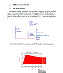
Untitled3.png
what is the problem?
using spice model in this simulation is wrong?

Best Regards.
 

SPICE model sounds right, but is your gate and drain voltage correct?

First of all thanks for your answer.
I saw datasheet again. for I-V curve Vgs is 6 to 16 volt and the drain voltage is 12.5 volt. Next I simulate the spice model with Vgs from 6 to 16 and these warnings are detected:

Warning detected by hpeesofsim during DC analysis `DC1'.
Circuit converged with at least one device's P-N junction current
exceeding the explosion current and junction has been linearized.
You may want to increase the explosion current in the device model or in
the Options (if the parameter is not given in the model) and resimulate.
You may need to increase Maximum number of warnings under Output tab
in Options to see which devices have been linearized.
Warning detected by hpeesofsim during DC analysis `DC1'.
Diode `X1.dbody' explosion current exceeded.
Warning detected by hpeesofsim during DC analysis `DC1'.
JFET `X1.jfet' explosion current exceeded.

I increase Imax and Imelt of the models to 3A but nothing happened.
here is my datasheet **broken link removed**

what should I do ???

thanks alot.
 

Vgs is given being as 6 to 16 V.I think it's too much and there is a mistake in the datasheet Vds vs. Ids ( Vgs param.)curve.
 

Vgs is given being as 6 to 16 V.I think it's too much and there is a mistake in the datasheet Vds vs. Ids ( Vgs param.)curve.

Thanks dear Bigboss
I check another transistor with 5 W output power and Vgs is 6 to 20 volt.
now I have a question. in class AB pwer amplifier Vgs is less than Vth. and for my transistor Vth min is 1 volt. then how should I bias this transistor according to the given Vgs in datasheet ?

thanks alot.
 

Status
Not open for further replies.

Similar threads

Part and Inventory Search

Welcome to EDABoard.com

Sponsor

Back
Top