Continue to Site

Welcome to EDAboard.com

Welcome to our site! EDAboard.com is an international Electronics Discussion Forum focused on EDA software, circuits, schematics, books, theory, papers, asic, pld, 8051, DSP, Network, RF, Analog Design, PCB, Service Manuals... and a whole lot more! To participate you need to register. Registration is free. Click here to register now.

BFP420 CE Amplifier Gain

Status
Not open for further replies.

aht2000

Junior Member level 3
Joined
Apr 18, 2015
Messages
30
Helped
0
Reputation
0
Reaction score
2
Trophy points
1,288
Activity points
1,664
Hi,
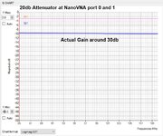
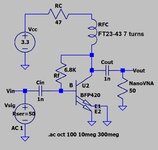
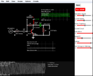
Sorry for the long post, but I am trying to verify my understanding with the experts on how the gain of the attached circuit (schematic attached) is calculated. I built the actual circuit on a PCB and measured its gain in the FM Band using a NanoVNA, and it shows 30db flat power gain (S21) taking into consideration the 20db attenuators installed on both ports of the nanoVNA (screen shot shows -10db).

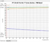
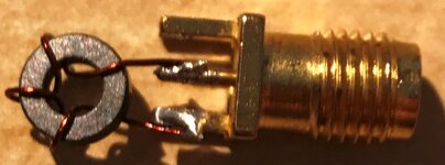
My understanding is the gain of the common emitter amplifier is Rc over Re (hope this holds true in the RF world too). In this case, I assume Rc is 47 ohm + impedance of RFC. I measured the S11 RFC alone using the NanoVNA (screen shot attached), and it is around 850 ohm of resistance. and 250 ohm of reactance ( |Z| = 900 ohm)

With Ic = 18mA, so Re = VT/18 = 1.3 ohm. I would expect the voltage gain to be (900+47)/1.3 = 728.

However as the output load is 50 ohm (port 1 of the nanoVNA), then I was expecting the above calculated gain to drop to 728* 50/(900+47) = 38.

Looking at the nanoVNA S21, it is 30db of power gain. if I calculate the same power gain based on the calculated voltage gain, it would be 20 log 38 = 31.6db with 1.6db deviation.

If I remove the RFC, then I assume that the RC is now only 47 ohm. So, the gain would be 47/1.3 = 36. As the output impedance is now 47 ohm almost equal to the 50 ohm load, so, I would expect the gain to drop by half to be 18.

And the power gain would be 20 log 18 = 25db.

So, the benefit of the RFC is that it gave me 5db more in power gain. Is this the case, or am I missing something? At the same time, it caused the output impedance and gain to be frequency dependent, and the output impedance became far higher than the typical target 50 ohm in RF.
I assume that the real benefit of the RFC comes when I am building a narrow band amplifier at which case I can build an LC matching network to match the amplifier output impedance to the 50 ohm load.

I sometime see in other schematics a capacitor connected from the point between the RFC and 47 ohm to ground. I assume that this is a bypass capacitor to prevent any RF who passed through the RFC to reach the power supply and its value should be chosen so that its impedance at the minimum frequency of interest at least 10 times less than the 47 ohm, and it does not cause a series resonance with the RFC anywhere in the amplifier band of interest.

Thank you.
 

Attachments

  • S21 Gain with 40db external attenuator.jpg
    S21 Gain with 40db external attenuator.jpg
    331 KB · Views: 128
  • FT23-43 Series RLC FM band.jpg
    FT23-43 Series RLC FM band.jpg
    314.1 KB · Views: 136
  • Schematic.jpg
    Schematic.jpg
    89.2 KB · Views: 211

The inductance of FT23-47 with 7 turns is about 8uH.
So at 100 MHz the reactance of the 8uH choke is 5 kilo ohms.

Usually the reactance of an RF choke should be 10x greater than the impedance of the circuit, so for 50 ohm situation should be 500 ohms. In your case, the FT23-47 toroid should have about 2.5 turns which means about 800nH.

With 800nH choke LTspice shows flat gain of 28dB between 85MHz and 110MHz.
 

The design/essay is completely wrong from A to Z..
You should work on RF Design Techniques because RF designing is completely different.
 

The inductance of FT23-47 with 7 turns is about 8uH.
So at 100 MHz the reactance of the 8uH choke is 5 kilo ohms.

Usually the reactance of an RF choke should be 10x greater than the impedance of the circuit, so for 50 ohm situation should be 500 ohms. In your case, the FT23-47 toroid should have about 2.5 turns which means about 800nH.

With 800nH choke LTspice shows flat gain of 28dB between 85MHz and 110MHz.
I tried 2.5 (in fact 3 turns) as I already suffered with the 7 turns and for some reason at relatively low frequency the inductance is around what the toroid.info provides. However as the frequency increases, the calculated inductance by the nanoVNA seems to drop. I am attaching a photo of the winding as well as the series RLC equivalent at different frequency ranges. Is this right way to wind the toroid? Is there anything else that interfere to make the inductance shows as decreasing as the frequency increases?
--- Updated ---

The design/essay is completely wrong from A to Z..
You should work on RF Design Techniques because RF designing is completely different.
Thank you, will look into s-parameters way of doing things.
 

Attachments

  • FT23-43 Ferrite Bead 3 Turns Impedance with frequency.JPG
    FT23-43 Ferrite Bead 3 Turns Impedance with frequency.JPG
    341.7 KB · Views: 88
  • FT23-43 Ferrite Bead 3 Turns.JPG
    FT23-43 Ferrite Bead 3 Turns.JPG
    174.1 KB · Views: 91

First I wondered if the VNA measurement might have failed due to incorrectly calibrated reference plane. Then I looked at material 43 data sheet, specifically complex permeability curves. It shows a crossing of u' and u" at about 15 MHz similar to your impedance measurement. Thus I think, the inductance drop is according to actual ferrite core properties.

20211021_225625.jpg
 

You should not expect more than 30 dB gain as this has negative feedback. (Rfb/Rs=6k8/50=136 ignoring 1nF) on an open loop gain (Aol = Zc / (Re+rbe) which is not enough open loop gain to achieve more than 30 dB gain without a lot of harmonic distortion from asymmetric current gain. You could change the collector 50+RFC to 100 nH for 300 MHz for an almost equivalent 50 ohms reactance without the resistor and get almost the same gain. Negative feedback CE config's will reduce nonlinearity by reduce Vbe variation and will be improved by cascading stages with lower gain or adding 1 ohm emitter Re for improve linearity. I don't know your specs you want for THD or 3OI but reducing your gain expectations with more current gain and linear feedback and adding linear R equal to the dynamic resistance is what I suggest.

My rule of thumb is to expect 50% of Rfb/ Rs for high Aol unless exceptionally high hFE such as a Darlington or cascode.
 

First I wondered if the VNA measurement might have failed due to incorrectly calibrated reference plane. Then I looked at material 43 data sheet, specifically complex permeability curves. It shows a crossing of u' and u" at about 15 MHz similar to your impedance measurement. Thus I think, the inductance drop is according to actual ferrite core properties.

View attachment 172494
As the reactance of the RFC falls with frequency, from the VNA measurements, the resistive part increases. Back to vfone response "Usually the reactance of an RF choke should be 10x greater than the impedance of the circuit," my modest understanding that the purpose of the RFC in my schematic is to block the DC biasing from the AC path. So can I rely accordingly on the overall Z of the RFC being mainly resistive at this 100MHz range or it has to be reactance nature to meet his point?
 

You should not expect more than 30 dB gain as this has negative feedback. (Rfb/Rs=6k8/50=136 ignoring 1nF) on an open loop gain (Aol = Zc / (Re+rbe) which is not enough open loop gain to achieve more than 30 dB gain without a lot of harmonic distortion from asymmetric current gain. You could change the collector 50+RFC to 100 nH for 300 MHz for an almost equivalent 50 ohms reactance without the resistor and get almost the same gain. Negative feedback CE config's will reduce nonlinearity by reduce Vbe variation and will be improved by cascading stages with lower gain or adding 1 ohm emitter Re for improve linearity. I don't know your specs you want for THD or 3OI but reducing your gain expectations with more current gain and linear feedback and adding linear R equal to the dynamic resistance is what I suggest.

My rule of thumb is to expect 50% of Rfb/ Rs for high Aol unless exceptionally high hFE such as a Darlington or cascode.
If I remove the 50 ohm in the Vcc to collector path (replace it with equivalent reactance), wouldn't this disturb the DC biasing of the transistor and increases the Ic dramatically?
 

You still control the current with Rfb but, yes you change the bias current with a base pull up or down. I chose a negative supply here for direct coupling the output at 0V. There are better ways than this example.


I hope you can read my plots and change the component values with your mouse wheel or tap properties.

Pulling off load resistor gives a gain around 52 then loaded gain ~ 21 with 10mVpp input
--- Updated ---

Notice I reduced gain to get more linearity with Re= 0.6 ohms which is larger than rbe.

Notice how negative feedback reduces the input by 60% from 10mVpp to 4mVpp thus reducing gain but improving linearity. since gm or rbe is modulated by Vbe and changes the peak gain for pos and neg peaks
 
Last edited:

Here's another Av=20 = 30 dB gain but reducing sweep range 100~300 MHz to show you a trick I use to measure THD.

The percentage peak asymmetry of a sinusoid is the cause of all harmonics and correlates well with est

%THD = \( \dfrac{V_{max}-V_{min}} {Vpp} \)

example: Vcc= 3.3 , Input = 50R+ 1nF, Feedback Rcb= 4k was determine when Vbe(AC) was 50% of Vin before the 50 Ohms which means expected good s11 input match.

This resulted in Rce/Rin = 80 with Re=750 mohm with an arbitrary hFE= 78

Base input impedance open loop is Rin= hFE*(rbe+Re) while negative feedback ratio lowers both input and output impedance , so the Rcb was adjust to match 50 ohms and have a feedback ratio with Re to create a matched input. (But this is also affected by Lc and load R. with the collector current source to the feedback resistor.)

observing probe Vpp on output stopped at 299 MHz, the unloaded input = 100 mVpp, Vout= 1.92Vpp Av=19.2 , Vbe=50.5mVpp
The plot in top right now is the 50 ohm load coupled by 1nF shows Min= -981.63 , Max = 940.67 mV
Thus from my THD formula ... (981-940) / 1920 *100% = 2.1%

Now when I increase base bias with 10k Base to Vcc=3.3V
the input Z drops to 47 mV /100 the Vbe increases with Ic and reduces rbe increasing gm and gain to from 19.2 to 20.4 with Min=1.01, Max=1.03 Out=2.04Vpp thus THD = 20mV/2.04V = 1% just from raising the bias current and Vbe rise of a couple mV.

if lower THD was desired, then tweaks to increase open loop gain are needed and thus more feedback ratio to linearize with the tradeoff of gain or power consumption.
--- Updated ---

Please Note that my THD formula is only for AC coupled signals with a stable 0Vdc.

1634916430105.png
 

Attachments

  • 1634914921138.png
    1634914921138.png
    141.5 KB · Views: 88
Last edited:

Here's another Av=20 = 30 dB gain but reducing sweep range 100~300 MHz to show you a trick I use to measure THD.

The percentage peak asymmetry of a sinusoid is the cause of all harmonics and correlates well with est

%THD = \( \dfrac{V_{max}-V_{min}} {Vpp} \)

example: Vcc= 3.3 , Input = 50R+ 1nF, Feedback Rcb= 4k was determine when Vbe(AC) was 50% of Vin before the 50 Ohms which means expected good s11 input match.

This resulted in Rce/Rin = 80 with Re=750 mohm with an arbitrary hFE= 78

Base input impedance open loop is Rin= hFE*(rbe+Re) while negative feedback ratio lowers both input and output impedance , so the Rcb was adjust to match 50 ohms and have a feedback ratio with Re to create a matched input. (But this is also affected by Lc and load R. with the collector current source to the feedback resistor.)

observing probe Vpp on output stopped at 299 MHz, the unloaded input = 100 mVpp, Vout= 1.92Vpp Av=19.2 , Vbe=50.5mVpp
The plot in top right now is the 50 ohm load coupled by 1nF shows Min= -981.63 , Max = 940.67 mV
Thus from my THD formula ... (981-940) / 1920 *100% = 2.1%

Now when I increase base bias with 10k Base to Vcc=3.3V
the input Z drops to 47 mV /100 the Vbe increases with Ic and reduces rbe increasing gm and gain to from 19.2 to 20.4 with Min=1.01, Max=1.03 Out=2.04Vpp thus THD = 20mV/2.04V = 1% just from raising the bias current and Vbe rise of a couple mV.

if lower THD was desired, then tweaks to increase open loop gain are needed and thus more feedback ratio to linearize with the tradeoff of gain or power consumption.
--- Updated ---

Please Note that my THD formula is only for AC coupled signals with a stable 0Vdc.

View attachment 172506
Thank you very much SunnySkyguy for your comprehensive answer. I didn't come across this online simulator before, seems very interesting.
 
Status
Not open for further replies.

Part and Inventory Search

Welcome to EDABoard.com

Sponsor

Back
Top