new_rf_engineer
Newbie
Hi,
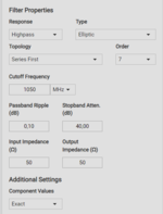
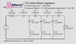
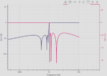
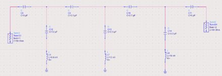
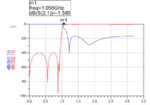
I am new in RF electronics. I am learning ADS and other theoretical stuff about RF. I thought that i can create an Elliptic LC high pass filter on real PCB board to exercise. Before i create the board, firstly, i have chosen a high pass cut off frequency from RF-tools website. The specs, circuit schematic and graph can be seen in Fig. 1, Fig. 2, and Fig. 3 respectively. The cut off frequency which i have chosen is 1050 MHz. Then, to see the same figure in ADS, I simulated the fig2 schematic in ADS. In the ADS simulation, i used the standard component values for capacitors and inductors by rounding the exact values from RF Tools schematic. This circuit schematic and graph can be seen in Fig. 4 and Fig. 5. respectively. In the next step, Because I am going to use my real components on board, I had to make a realistic simulation. I have the capacitors and inductors with SMD 603. I added them to ADS as C_pad1 and L_pad1. Also, I attached the microstrip lines to the ADS.
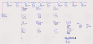
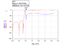
Finally, the microstrip lines and 3d components(SMD 603 capacitor and inductor) are ready and same with the board. This circuit schematic can be seen in Fig. 6 and corresponding graph in Fig. 7. As it can be seen in Fig7, the cut off frequency is not the same which i selected at first and i think that this is due to the lines. The graph in fig.7 is my expectation on Real PCB.
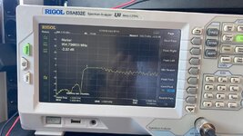
I created the same circuit with the same lines on PCB. The lines and components are the same with the ADS in PCB. After i observe the graph of this PCB in spectrum analyzer, i got the graph in fig. 8. From now on, I told you the step by step implementation of a high pass LC filter by me. The graph is totally different and cut off frequency is about 954 MHz instead of 1050 Mhz which i have chosen at the first. PCB is very small and it contains only the necessary components in the circuit from fig. 6. The PCB has FR-4 material.
Why ads simulation and pcb implementation is too different ? Do i make something wrong in ADS? What points do i need to check to distinguish failure?
Thanks in advance
I am new in RF electronics. I am learning ADS and other theoretical stuff about RF. I thought that i can create an Elliptic LC high pass filter on real PCB board to exercise. Before i create the board, firstly, i have chosen a high pass cut off frequency from RF-tools website. The specs, circuit schematic and graph can be seen in Fig. 1, Fig. 2, and Fig. 3 respectively. The cut off frequency which i have chosen is 1050 MHz. Then, to see the same figure in ADS, I simulated the fig2 schematic in ADS. In the ADS simulation, i used the standard component values for capacitors and inductors by rounding the exact values from RF Tools schematic. This circuit schematic and graph can be seen in Fig. 4 and Fig. 5. respectively. In the next step, Because I am going to use my real components on board, I had to make a realistic simulation. I have the capacitors and inductors with SMD 603. I added them to ADS as C_pad1 and L_pad1. Also, I attached the microstrip lines to the ADS.
Finally, the microstrip lines and 3d components(SMD 603 capacitor and inductor) are ready and same with the board. This circuit schematic can be seen in Fig. 6 and corresponding graph in Fig. 7. As it can be seen in Fig7, the cut off frequency is not the same which i selected at first and i think that this is due to the lines. The graph in fig.7 is my expectation on Real PCB.
I created the same circuit with the same lines on PCB. The lines and components are the same with the ADS in PCB. After i observe the graph of this PCB in spectrum analyzer, i got the graph in fig. 8. From now on, I told you the step by step implementation of a high pass LC filter by me. The graph is totally different and cut off frequency is about 954 MHz instead of 1050 Mhz which i have chosen at the first. PCB is very small and it contains only the necessary components in the circuit from fig. 6. The PCB has FR-4 material.
Why ads simulation and pcb implementation is too different ? Do i make something wrong in ADS? What points do i need to check to distinguish failure?
Thanks in advance