Continue to Site

Welcome to EDAboard.com

Welcome to our site! EDAboard.com is an international Electronics Discussion Forum focused on EDA software, circuits, schematics, books, theory, papers, asic, pld, 8051, DSP, Network, RF, Analog Design, PCB, Service Manuals... and a whole lot more! To participate you need to register. Registration is free. Click here to register now.

[SOLVED] Are my components called incorrectly?

Status
Not open for further replies.

GreatField

Newbie level 6
Joined
Mar 13, 2022
Messages
13
Helped
0
Reputation
0
Reaction score
0
Trophy points
1
Activity points
109
My code compiles perfectly in quartus II, but when simulating in the waveform it seems that the components are not being used because nothing happens in the simulation.


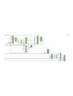
See my RTL Viewer:
0001.jpg


See my code:


Code:
LIBRARY ieee;
USE ieee.std_logic_1164.all;
USE IEEE.numeric_std.all;

LIBRARY work;

ENTITY Projeto IS
    PORT
    (
        --GND : IN STD_LOGIC;
        dados_entrada    : INOUT unsigned (7 downto 0);
        enderecamento : INOUT unsigned (3 downto 0);
        dados_de_saida : INOUT unsigned (7 downto 0);
        leitura :  INOUT  std_logic;
        Clock_mem :  INOUT  std_logic;
        Clock_reg_RDM :  INOUT  std_logic;
        Clock_reg_RI :  INOUT  std_logic;
        bit_selector_mux1 : INOUT std_logic;
        saida_reg_RI : INOUT unsigned (7 downto 0)
    );
END Projeto;

ARCHITECTURE top_lvl_entity OF Projeto IS


COMPONENT registrador_REM IS
    PORT
    (
        CLOCK, D0, D1, D2, D3, D4, D5, D6, D7 :  INOUT  STD_LOGIC;
        Q0, Q1, Q2, Q3, Q4, Q5, Q6, Q7 :  BUFFER  STD_LOGIC      
    );
END COMPONENT registrador_REM;


COMPONENT registrador_RDM IS
    PORT
    (
        CLK, D8, D9, D10, D11, D12, D13, D14, D15 :  INOUT  STD_LOGIC;
        Q8, Q9, Q10, Q11, Q12, Q13, Q14, Q15 :  BUFFER  STD_LOGIC  
    );
END COMPONENT registrador_RDM;


COMPONENT registrador_RI IS
    PORT
    (
        C_L_K, D16, D17, D18, D19, D20, D21, D22, D23 :  INOUT  STD_LOGIC;
        Q16, Q17, Q18, Q19, Q20, Q21, Q22, Q23 :  BUFFER  STD_LOGIC      
    );
END COMPONENT registrador_RI;


COMPONENT registrador_AC IS
    PORT
    (
        C_L_O_C_K, D24, D25, D26, D27, D28, D29, D30, D31 :  INOUT  STD_LOGIC;
        Q24, Q25, Q26, Q27, Q28, Q29, Q30, Q31 :  BUFFER  STD_LOGIC  
    );
END COMPONENT registrador_AC;


COMPONENT mux_1 IS
    PORT
    (
        A0 :  INOUT  STD_LOGIC;
        B0 :  INOUT  STD_LOGIC;
        A1 :  INOUT  STD_LOGIC;
        B1 :  INOUT  STD_LOGIC;
        A2 :  INOUT  STD_LOGIC;
        B2 :  INOUT  STD_LOGIC;
        A3 :  INOUT  STD_LOGIC;
        B3 :  INOUT  STD_LOGIC;
        A4 :  INOUT  STD_LOGIC;
        B4 :  INOUT  STD_LOGIC;
        A5 :  INOUT  STD_LOGIC;
        B5 :  INOUT  STD_LOGIC;
        A6 :  INOUT  STD_LOGIC;
        B6 :  INOUT  STD_LOGIC;
        A7 :  INOUT  STD_LOGIC;
        B7 :  INOUT  STD_LOGIC;
        bit_controle :  INOUT  STD_LOGIC;
        S1 :  INOUT  STD_LOGIC;
        S2 :  INOUT  STD_LOGIC;
        S3 :  INOUT  STD_LOGIC;
        S4 :  INOUT  STD_LOGIC;
        S5 :  INOUT  STD_LOGIC;
        S6 :  INOUT  STD_LOGIC;
        S7 :  INOUT  STD_LOGIC;
        S8 :  INOUT  STD_LOGIC
    );
END COMPONENT mux_1;


COMPONENT mux_2 IS
    PORT
    (
        C0 :  INOUT  STD_LOGIC;
        F0 :  INOUT  STD_LOGIC;
        C1 :  INOUT  STD_LOGIC;
        F1 :  INOUT  STD_LOGIC;
        C2 :  INOUT  STD_LOGIC;
        F2 :  INOUT  STD_LOGIC;
        C3 :  INOUT  STD_LOGIC;
        F3 :  INOUT  STD_LOGIC;
        C4 :  INOUT  STD_LOGIC;
        F4 :  INOUT  STD_LOGIC;
        C5 :  INOUT  STD_LOGIC;
        F5 :  INOUT  STD_LOGIC;
        C6 :  INOUT  STD_LOGIC;
        F6 :  INOUT  STD_LOGIC;
        C7 :  INOUT  STD_LOGIC;
        F7 :  INOUT  STD_LOGIC;
        bit_ctrl :  INOUT  STD_LOGIC;
        G1 :  INOUT  STD_LOGIC;
        G2 :  INOUT  STD_LOGIC;
        G3 :  INOUT  STD_LOGIC;
        G4 :  INOUT  STD_LOGIC;
        G5 :  INOUT  STD_LOGIC;
        G6 :  INOUT  STD_LOGIC;
        G7 :  INOUT  STD_LOGIC;
        G8 :  INOUT  STD_LOGIC
    );
END COMPONENT mux_2;


COMPONENT decoder_4x8 IS
    PORT
    (
        B :  INOUT  STD_LOGIC;
        A :  INOUT  STD_LOGIC;
        C :  INOUT  STD_LOGIC;
        D :  INOUT  STD_LOGIC;
        O1 :  INOUT  STD_LOGIC;
        O2 :  INOUT  STD_LOGIC;
        O3 :  INOUT  STD_LOGIC;
        O4 :  INOUT  STD_LOGIC;
        O5 :  INOUT  STD_LOGIC;
        O6 :  INOUT  STD_LOGIC;
        O7 :  INOUT  STD_LOGIC;
        O8 :  INOUT  STD_LOGIC
    );
END COMPONENT decoder_4x8;


COMPONENT memoria_16x8 IS
    PORT
    (  
        address : INOUT unsigned (3 downto 0);
        data_in : INOUT unsigned (7 downto 0);
        data_out : INOUT unsigned (7 downto 0);
        RD :  INOUT  std_logic;
        CS :  INOUT  std_logic

    );
END COMPONENT memoria_16x8;


--      SIGNALS
signal t1 : std_logic;
signal t2 : std_logic;
signal t3 : std_logic;
signal t4 : std_logic;
signal t5 : std_logic;
signal t6 : std_logic;
signal t7 : std_logic;
signal t8 : std_logic;

signal t9 : std_logic;
signal t10 : std_logic;
signal t11 : std_logic;
signal t12 : std_logic;
signal t13 : std_logic;
signal t14 : std_logic;
signal t15 : std_logic;
signal t16 : std_logic;

signal t17 : std_logic;
signal t18 : std_logic;
signal t19 : std_logic;
signal t20 : std_logic;
signal t21 : std_logic;
signal t22 : std_logic;
signal t23 : std_logic;
signal t24 : std_logic;

signal t25 : std_logic;
signal t26 : std_logic;
signal t27 : std_logic;
signal t28 : std_logic;
signal t29 : std_logic;
signal t30 : std_logic;
signal t31 : std_logic;
signal t32 : std_logic;  

signal t33 : std_logic;
signal t34 : std_logic;
signal t35 : std_logic;
signal t36 : std_logic;
signal t37 : std_logic;
signal t38 : std_logic;
signal t39 : std_logic;
signal t40 : std_logic;

signal t41 : std_logic;
signal t42 : std_logic;
signal t43 : std_logic;
signal t44 : std_logic;

signal t45 : std_logic;
signal t46 : std_logic;
signal t47 : std_logic;
signal t48 : std_logic;

signal t49 : std_logic;
signal t50 : std_logic;
signal t51 : std_logic;
signal t52 : std_logic;

BEGIN


t25 <= dados_entrada(0);
t25 <= dados_entrada(1);
t25 <= dados_entrada(2);
t25 <= dados_entrada(3);
t25 <= dados_entrada(4);
t25 <= dados_entrada(5);
t25 <= dados_entrada(6);
t25 <= dados_entrada(7);

t41 <= enderecamento(0);
t42 <= enderecamento(1);
t43 <= enderecamento(2);
t44 <= enderecamento(3);

t1 <= dados_de_saida(0);
t2 <= dados_de_saida(1);
t3 <= dados_de_saida(2);
t4 <= dados_de_saida(3);
t5 <= dados_de_saida(4);
t6 <= dados_de_saida(5);
t7 <= dados_de_saida(6);
t8 <= dados_de_saida(7);


t45 <= saida_reg_RI(0);  
t46 <= saida_reg_RI(1);
t47 <= saida_reg_RI(2);
t48 <= saida_reg_RI(3);
t49 <= saida_reg_RI(4);
t50 <= saida_reg_RI(5);
t51 <= saida_reg_RI(6);
t52 <= saida_reg_RI(7);


P1: memoria_16x8
    port map(
        --SIGNALS
        address(0) => t41,
        address(1) => t42,
        address(2) => t43,
        address(3) => t44,
        data_out(0) => t1,
        data_out(1) => t2,
        data_out(2) => t3,
        data_out(3) => t4,
        data_out(4) => t5,
        data_out(5) => t6,
        data_out(6) => t7,
        data_out(7) => t8,
        data_in(0) => t25,
        data_in(1) => t26,
        data_in(2) => t27,
        data_in(3) => t28,
        data_in(4) => t29,
        data_in(5) => t30,
        data_in(6) => t31,
        data_in(7) => t32,
        CS => Clock_mem,
        RD => leitura
    );
   
   
P2: registrador_AC
    port map(
        Q24 => t9,
        Q25 => t10,
        Q26 => t11,
        Q27 => t12,
        Q28 => t13,
        Q29 => t14,
        Q30 => t15,
        Q31 => t16
    );


P3: mux_1
    port map(
        -- SIGNALS
        A0 => t1,
        B0 => t2,
        A1 => t3,
        B1 => t4,
        A2 => t5,
        B2 => t6,
        A3 => t7,
        B3 => t8,
        A4 => t9,
        B4 => t10,
        A5 => t11,
        B5 => t12,
        A6 => t13,
        B6 => t14,
        A7 => t15,
        B7 => t16,
        S1    => t17,
        S2 => t18,
        S3 => t19,
        S4 => t20,
        S5 => t21,
        S6 => t22,
        S7 => t23,
        S8 => t24,
        bit_controle => bit_selector_mux1
    );

   
P4: registrador_RDM
    port map(
        --SIGNALS
        D8 => t17,
        D9 => t18,
        D10 => t19,
        D11 => t20,
        D12 => t21,
        D13 => t22,
        D14 => t23,
        D15 => t24,
        Q8 => t25,
        Q9 => t26,
        Q10 => t27,
        Q11 => t28,
        Q12 => t29,
        Q13 => t30,
        Q14 => t31,
        Q15 => t32,
        CLK => Clock_reg_RDM
       
    );
   
   
P8: mux_2
    port map(
        --SIGNALS
        C0 => t25,
        F0 => t26,
        C1 => t27,
        F1 => t28,
        C2 => t29,
        F2 => t30,
        C3 => t31,
        F3 => t32,
        C4 => t25,
        F4 => t26,
        C5 => t27,
        F5 => t28,
        C6 => t29,
        F6 => t30,
        C7 => t31,
        F7 => t32,
        G1 => t33,
        G2 => t34,
        G3 => t35,
        G4 => t36,
        G5 => t37,
        G6 => t38,
        G7 => t39,
        G8 => t40
    );
   
   
P9: registrador_REM  
    port map(
        --SIGNALS
        D0 => t33,
        D1 => t34,
        D2 => t35,
        D3 => t36,
        D4 => t37,
        D5 => t38,
        D6 => t39,
        D7 => t40,
        Q0 => t41,
        Q1 => t42,
        Q2 => t43,
        Q3 => t44  
    );
   
   
P10: registrador_RI
    port map(
        Q16 => t45,
        Q17 => t46,
        Q18 => t47,
        Q19 => t48,
        Q20 => t49,
        Q21 => t50,
        Q22 => t51,
        Q23 => t52,
        D16 => t25,
        D17 => t26,
        D18 => t27,
        D19 => t28,
        D20 => t29,
        D21 => t30,
        D22 => t31,
        D23 => t32,
       C_L_K => Clock_reg_RI
       
    );

P11: decoder_4x8
    port map(
        --SIGNALS
        A => t45,
        B => t46,
        C => t47,
        D => t48
    );

END top_lvl_entity;
 
Last edited by a moderator:
Just because it compiles doesn't mean it's going to do what you expect or want it to do. It only means there are no errors.

You have a whole bunch of components declared, but we have no idea what they are; they could be empty as far as we know.

Look at your synthesis/implementation reports and see if there are any clues there. Look at your implemented design.

Don't just tell us "nothing happens". SOMETHING happens; even an undefined output is something. Maybe your test bench is faulty. Maybe you don't initialize some things you need to initialize. Does your simulation show the input stimulus? Follow the stimulus signal through the chain and see where it breaks.
 

all component is work perfectly
All components work perfectly.
They just don't work when called via "component" on my top level entity.

I found this error and fixed it but the error persists.

t25 <= dados_entrada(0);
t25 <= dados_entrada(1);
t25 <= dados_entrada(2);
t25 <= dados_entrada(3);
t25 <= dados_entrada(4);
t25 <= dados_entrada(5);
t25 <= dados_entrada(6);
t25 <= dados_entrada(7);

Analysing the folder

Code:
Warning (10036): Verilog HDL or VHDL warning at Projeto_Neander.vhd(230): object "t49" assigned a value but never read
Warning (10036): Verilog HDL or VHDL warning at Projeto_Neander.vhd(231): object "t50" assigned a value but never read
Warning (10036): Verilog HDL or VHDL warning at Projeto_Neander.vhd(232): object "t51" assigned a value but never read
Warning (10036): Verilog HDL or VHDL warning at Projeto_Neander.vhd(233): object "t52" assigned a value but never read


Warning (12161): Node "registrador_AC:p2|D31" is stuck at GND because node is in wire loop and does not have a source
Warning (12161): Node "registrador_AC:p2|D30" is stuck at GND because node is in wire loop and does not have a source
Warning (12161): Node "registrador_AC:p2|D29" is stuck at GND because node is in wire loop and does not have a source
Warning (12161): Node "registrador_AC:p2|D28" is stuck at GND because node is in wire loop and does not have a source
Warning (12161): Node "registrador_AC:p2|D27" is stuck at GND because node is in wire loop and does not have a source
Warning (12161): Node "registrador_AC:p2|D26" is stuck at GND because node is in wire loop and does not have a source
Warning (12161): Node "registrador_AC:p2|D25" is stuck at GND because node is in wire loop and does not have a source
Warning (12161): Node "registrador_AC:p2|D24" is stuck at GND because node is in wire loop and does not have a source
Warning (12161): Node "mux_2:p8|bit_ctrl" is stuck at GND because node is in wire loop and does not have a source

Warning (12241): 8 hierarchies have connectivity warnings - see the Connectivity Checks report folder

Warning (13039): The following bidirectional pins have no drivers
    Warning (13040): bidirectional pin "dados_entrada[7]" has no driver
    Warning (13040): bidirectional pin "dados_entrada[6]" has no driver
    Warning (13040): bidirectional pin "dados_entrada[5]" has no driver
    Warning (13040): bidirectional pin "dados_entrada[4]" has no driver
    Warning (13040): bidirectional pin "dados_entrada[3]" has no driver
    Warning (13040): bidirectional pin "dados_entrada[2]" has no driver
    Warning (13040): bidirectional pin "dados_entrada[1]" has no driver
    Warning (13040): bidirectional pin "dados_entrada[0]" has no driver
    Warning (13040): bidirectional pin "enderecamento[3]" has no driver
    Warning (13040): bidirectional pin "enderecamento[2]" has no driver
    Warning (13040): bidirectional pin "enderecamento[1]" has no driver
    Warning (13040): bidirectional pin "enderecamento[0]" has no driver
    Warning (13040): bidirectional pin "dados_de_saida[7]" has no driver
    Warning (13040): bidirectional pin "dados_de_saida[6]" has no driver
    Warning (13040): bidirectional pin "dados_de_saida[5]" has no driver
    Warning (13040): bidirectional pin "dados_de_saida[4]" has no driver
    Warning (13040): bidirectional pin "dados_de_saida[3]" has no driver
    Warning (13040): bidirectional pin "dados_de_saida[2]" has no driver
    Warning (13040): bidirectional pin "dados_de_saida[1]" has no driver
    Warning (13040): bidirectional pin "dados_de_saida[0]" has no driver
    Warning (13040): bidirectional pin "leitura" has no driver
    Warning (13040): bidirectional pin "Clock_mem" has no driver
    Warning (13040): bidirectional pin "Clock_reg_RDM" has no driver
    Warning (13040): bidirectional pin "Clock_reg_RI" has no driver
    Warning (13040): bidirectional pin "bit_selector_mux1" has no driver
    Warning (13040): bidirectional pin "saida_reg_RI[3]" has no driver
    Warning (13040): bidirectional pin "saida_reg_RI[2]" has no driver
    Warning (13040): bidirectional pin "saida_reg_RI[1]" has no driver
    Warning (13040): bidirectional pin "saida_reg_RI[0]" has no driver
    Warning (13040): bidirectional pin "saida_reg_RI[4]" has no driver
    Warning (13040): bidirectional pin "saida_reg_RI[5]" has no driver
    Warning (13040): bidirectional pin "saida_reg_RI[6]" has no driver
    Warning (13040): bidirectional pin "saida_reg_RI[7]" has no driver


I checked the "Connectivity Checks report folder" and found several errors like this on each port of my components:

Connected to dangling logic. Logic that only feeds a dangling port will be removed.
 
Last edited by a moderator:

Your design generates no output, the only potential output, bidirectional port saida_reg_RI is nowhere driven.

Reconsider what you have written. Is the RTL schematic basically representing what you intend? Where should the output be connected in the schematic, why is it missing in the VHDL code?
 

Your design generates no output, the only potential output, bidirectional port saida_reg_RI is nowhere driven.

Reconsider what you have written. Is the RTL schematic basically representing what you intend? Where should the output be connected in the schematic, why is it missing in the VHDL code?

I removed all output from the project and replaced it with "INOUT" because it gave a series of errors like "a port of type IN cannot be assigned to a port of type OUT".

This error disappeared when I switched to INOUT


I removed the components and brought their code to the top level entity of the project.
I'm just having trouble connecting ports.
I've tried in several possible ways with signals and it gives several errors.
I'm new to vhdl
See the new code below:


Code:
LIBRARY ieee;
USE ieee.std_logic_1164.all;
USE IEEE.numeric_std.all;

LIBRARY work;

ENTITY Projeto IS
    PORT
    (
        
        CLOCK        :  IN  STD_LOGIC;
        D0, D1, D2, D3, D4, D5, D6, D7 :  INOUT  STD_LOGIC;
        Q0, Q1, Q2, Q3, Q4, Q5, Q6, Q7 :  BUFFER  STD_LOGIC;
        
        CLK    :  IN STD_LOGIC;
        D8, D9, D10, D11, D12, D13, D14, D15 :  INOUT  STD_LOGIC;
        Q8, Q9, Q10, Q11, Q12, Q13, Q14, Q15 :  BUFFER  STD_LOGIC;
        
        C_L_K            : IN STD_LOGIC;
        D16, D17, D18, D19, D20, D21, D22, D23 :  INOUT  STD_LOGIC;
        Q16, Q17, Q18, Q19, Q20, Q21, Q22, Q23 :  BUFFER  STD_LOGIC;
        
        C_L_O_C_K        :     IN        STD_LOGIC;
        D24, D25, D26, D27, D28, D29, D30, D31 :  INOUT  STD_LOGIC;
        Q24, Q25, Q26, Q27, Q28, Q29, Q30, Q31 :  BUFFER  STD_LOGIC;
        
        C0 :  INOUT  STD_LOGIC;
        F0 :  INOUT  STD_LOGIC;
        C1 :  INOUT  STD_LOGIC;
        F1 :  INOUT  STD_LOGIC;
        C2 :  INOUT  STD_LOGIC;
        F2 :  INOUT  STD_LOGIC;
        C3 :  INOUT  STD_LOGIC;
        F3 :  INOUT  STD_LOGIC;
        C4 :  INOUT  STD_LOGIC;
        F4 :  INOUT  STD_LOGIC;
        C5 :  INOUT  STD_LOGIC;
        F5 :  INOUT  STD_LOGIC;
        C6 :  INOUT  STD_LOGIC;
        F6 :  INOUT  STD_LOGIC;
        C7 :  INOUT  STD_LOGIC;
        F7 :  INOUT  STD_LOGIC;
        bit_ctrl :  INOUT  STD_LOGIC;
        G1 :  INOUT  STD_LOGIC;
        G2 :  INOUT  STD_LOGIC;
        G3 :  INOUT  STD_LOGIC;
        G4 :  INOUT  STD_LOGIC;
        G5 :  INOUT  STD_LOGIC;
        G6 :  INOUT  STD_LOGIC;
        G7 :  INOUT  STD_LOGIC;
        G8 :  INOUT  STD_LOGIC;
        
        A0 :  INOUT  STD_LOGIC;
        B0 :  INOUT  STD_LOGIC;
        A1 :  INOUT  STD_LOGIC;
        B1 :  INOUT  STD_LOGIC;
        A2 :  INOUT  STD_LOGIC;
        B2 :  INOUT  STD_LOGIC;
        A3 :  INOUT STD_LOGIC;
        B3 :  INOUT  STD_LOGIC;
        A4 :  INOUT  STD_LOGIC;
        B4 :  INOUT  STD_LOGIC;
        A5 :  INOUT  STD_LOGIC;
        B5 :  INOUT  STD_LOGIC;
        A6 :  INOUT  STD_LOGIC;
        B6 :     INOUT  STD_LOGIC;
        A7 :  INOUT  STD_LOGIC;
        B7 :  INOUT  STD_LOGIC;
        bit_controle :  IN STD_LOGIC;
        S1 :  INOUT  STD_LOGIC;
        S2 :  INOUT  STD_LOGIC;
        S3 :  INOUT  STD_LOGIC;
        S4 :  INOUT  STD_LOGIC;
        S5 :  INOUT  STD_LOGIC;
        S6 :  INOUT  STD_LOGIC;
        S7 :  INOUT  STD_LOGIC;
        S8 :  INOUT  STD_LOGIC;
        
        address : in unsigned (3 downto 0);
        data_in : INOUT unsigned (7 downto 0);
        data_out : INOUT unsigned (7 downto 0);
        RD :  IN  std_logic;
        CS :  IN  std_logic;
        --decoder
        B :  INOUT  STD_LOGIC;
        A :  INOUT  STD_LOGIC;
        C :  INOUT  STD_LOGIC;
        D :  INOUT  STD_LOGIC;
        O1 :  INOUT  STD_LOGIC;
        O2 :  INOUT  STD_LOGIC;
        O3 :  INOUT  STD_LOGIC;
        O4 :  INOUT  STD_LOGIC;
        O5 :  INOUT  STD_LOGIC;
        O6 :  INOUT  STD_LOGIC;
        O7 :  INOUT  STD_LOGIC;
        O8 :  INOUT  STD_LOGIC
        
    );
END Projeto;

ARCHITECTURE top_lvl_entity OF Projeto IS


type  mem  is array(0 to 15) of unsigned(7 downto 0);
signal memoria : mem;


--      SIGNALS
signal t1 : std_logic;
signal t2 : std_logic;
signal t3 : std_logic;
signal t4 : std_logic;
signal t5 : std_logic;
signal t6 : std_logic;
signal t7 : std_logic;
signal t8 : std_logic;

signal t9 : std_logic;
signal t10 : std_logic;
signal t11 : std_logic;
signal t12 : std_logic;
signal t13 : std_logic;
signal t14 : std_logic;
signal t15 : std_logic;
signal t16 : std_logic;

signal t17 : std_logic;
signal t18 : std_logic;
signal t19 : std_logic;
signal t20 : std_logic;
signal t21 : std_logic;
signal t22 : std_logic;
signal t23 : std_logic;
signal t24 : std_logic;

signal t25 : std_logic;
signal t26 : std_logic;
signal t27 : std_logic;
signal t28 : std_logic;
signal t29 : std_logic;
signal t30 : std_logic;
signal t31 : std_logic;
signal t32 : std_logic;   

signal t33 : std_logic;
signal t34 : std_logic;
signal t35 : std_logic;
signal t36 : std_logic;
signal t37 : std_logic;
signal t38 : std_logic;
signal t39 : std_logic;
signal t40 : std_logic;

signal t41 : std_logic;
signal t42 : std_logic;
signal t43 : std_logic;
signal t44 : std_logic;

signal t45 : std_logic;
signal t46 : std_logic;
signal t47 : std_logic;
signal t48 : std_logic;

signal t49 : std_logic;
signal t50 : std_logic;
signal t51 : std_logic;
signal t52 : std_logic;


signal t53 : std_logic;

signal t54 : std_logic;
signal t55 : std_logic;
signal t56 : std_logic;
signal t57 : std_logic;
signal t58 : std_logic;
signal t59 : std_logic;
signal t60 : std_logic;
signal t61 : std_logic;

signal t62 : std_logic;
signal t63 : std_logic;
signal t64 : std_logic;
signal t65 : std_logic;
signal t66 : std_logic;
signal t67 : std_logic;
signal t68 : std_logic;
signal t69 : std_logic;


BEGIN

--REM
    Q0 <= D0 when (CLOCK'EVENT and CLOCK = '1') else
    Q0;
    
    Q1 <= D1 when (CLOCK'EVENT and CLOCK = '1') else
    Q1;

    Q2 <= D2 when (CLOCK'EVENT and CLOCK = '1') else
    Q2;
    
    Q3 <= D3 when (CLOCK'EVENT and CLOCK = '1') else
    Q3;
    
    Q4 <= D4 when (CLOCK'EVENT and CLOCK = '1') else
    Q4;
    
    Q5 <= D5 when (CLOCK'EVENT and CLOCK = '1') else
    Q5;
    
    Q6 <= D6 when (CLOCK'EVENT and CLOCK = '1') else
    Q6;
    
    Q7 <= D7 when (CLOCK'EVENT and CLOCK = '1') else
    Q7;


--RDM
    Q8 <= D8 when (CLK'EVENT and CLK = '1') else
    Q8;
    
    Q9 <= D9 when (CLK'EVENT and CLK = '1') else
    Q9;
    
    Q10 <= D10 when (CLK'EVENT and CLK = '1') else
    Q10;
    
    Q11 <= D11 when (CLK'EVENT and CLK = '1') else
    Q11;
    
    Q12 <= D12 when (CLK'EVENT and CLK = '1') else
    Q12;
    
    Q13 <= D13 when (CLK'EVENT and CLK = '1') else
    Q13;
    
    Q14 <= D14 when (CLK'EVENT and CLK = '1') else
    Q14;
    
    Q15 <= D15 when (CLK'EVENT and CLK = '1') else
    Q15;
    
--RI
    Q16 <= D16 when (C_L_K'EVENT and C_L_K = '1') else
    Q16;
    
    Q17 <= D17 when (C_L_K'EVENT and C_L_K = '1') else
    Q17;
    
    Q18 <= D18 when (C_L_K'EVENT and C_L_K = '1') else
    Q18;
    
    Q19 <= D19 when (C_L_K'EVENT and C_L_K = '1') else
    Q19;
    
    Q20 <= D20 when (C_L_K'EVENT and C_L_K = '1') else
    Q20;
    
    Q21 <= D21 when (C_L_K'EVENT and C_L_K = '1') else
    Q21;
    
    Q22 <= D22 when (C_L_K'EVENT and C_L_K = '1') else
    Q22;
    
    Q23 <= D23 when (C_L_K'EVENT and C_L_K = '1') else
    Q23;

--AC
    Q24 <= D24 when (C_L_O_C_K'EVENT and C_L_O_C_K = '1') else
    Q24;
    
    Q25 <= D25 when (C_L_O_C_K'EVENT and C_L_O_C_K = '1') else
    Q25;
    
    Q26 <= D26 when (C_L_O_C_K'EVENT and C_L_O_C_K = '1') else
    Q26;
    
    Q27 <= D27 when (C_L_O_C_K'EVENT and C_L_O_C_K = '1') else
    Q27;
    
    Q28 <= D28 when (C_L_O_C_K'EVENT and C_L_O_C_K = '1') else
    Q28;
    
    Q29 <= D29 when (C_L_O_C_K'EVENT and C_L_O_C_K = '1') else
    Q29;
    
    Q30 <= D30 when (C_L_O_C_K'EVENT and C_L_O_C_K = '1') else
    Q30;
    
    Q31 <= D31 when (C_L_O_C_K'EVENT and C_L_O_C_K = '1') else
    Q31;
    
    
--MUX-2
G1 <= (C0 and (not bit_ctrl)) or (F0 and bit_ctrl);
G2 <= (C1 and (not bit_ctrl)) or (F1 and bit_ctrl);
G3 <= (C2 and (not bit_ctrl)) or (F2 and bit_ctrl);
G4 <= (C3 and (not bit_ctrl)) or (F3 and bit_ctrl);
G5 <= (C4 and (not bit_ctrl)) or (F4 and bit_ctrl);
G6 <= (C5 and (not bit_ctrl)) or (F5 and bit_ctrl);
G7 <= (C6 and (not bit_ctrl)) or (F6 and bit_ctrl);
G8 <= (C7 and (not bit_ctrl)) or (F7 and bit_ctrl);

--MUX-1
S1 <= (A0 and (not bit_controle)) or (B0 and bit_controle);
S2 <= (A1 and (not bit_controle)) or (B1 and bit_controle);
S3 <= (A2 and (not bit_controle)) or (B2 and bit_controle);
S4 <= (A3 and (not bit_controle)) or (B3 and bit_controle);
S5 <= (A4 and (not bit_controle)) or (B4 and bit_controle);
S6 <= (A5 and (not bit_controle)) or (B5 and bit_controle);
S7 <= (A6 and (not bit_controle)) or (B6 and bit_controle);
S8 <= (A7 and (not bit_controle)) or (B7 and bit_controle);

--Memoria
      process(CS, address)   
      begin
      
        if rising_edge(CS) then 
          if RD = '0' then memoria(to_integer(address)) <= data_in;
          end if;
         end if;
        
      end process;
      
      data_out <= memoria(to_integer(address));


--decoder
O1 <= (not A) and (not B);
O2 <= (not A) and B;
O3 <= A and (not B);
O4 <= A and B;
O5 <= (not C) and (not D);
O6 <= (not C) and D;
O7 <= C and (not D);
O8 <= C and D;


--************************************** signals **************************************


        t41 <= address(0);
        t42 <= address(1);
        t43 <= address(2);
        t44 <= address(3);

        t1 <= data_out(0);
        t2 <= data_out(1);
        t3 <= data_out(2);
        t4 <= data_out(3);
        t5 <= data_out(4);
        t6 <= data_out(5);
        t7 <= data_out(6);
        t8 <= data_out(7);

        t25 <= data_in(0);
        t26 <= data_in(1);
        t27 <= data_in(2);
        t28 <= data_in(3);
        t29 <= data_in(4);
        t30 <= data_in(5);
        t31 <= data_in(6);
        t32 <= data_in(7);


        t9 <= Q24;
        t10 <= Q25;
        t11 <= Q26;
        t12 <= Q27;
        t13 <= Q28;
        t14 <= Q29;
        t15 <= Q30;
        t16 <= Q31;


        -- SIGNALS
        t1 <= A0;
        t2 <= B0;
        t3 <= A1;
        t4 <= B1;
        t5 <= A2;
        t6 <= B2;
        t7 <= A3;
        t8 <= B3;
        t9 <= A4;
        t10 <= B4;
        t11 <= A5;
        t12 <= B5;
        t13 <= A6;
        t14 <= B6;
        t15 <= A7;
        t16 <= B7;

        t17 <= S1;
        t18 <= S2;
        t19 <= S3;
        t20 <= S4;
        t21 <= S5;
        t22 <= S6;
        t23 <= S7;
        t24 <= S8;


        t17 <= D8;
        t18 <= D9;
        t19 <= D10;
        t20 <= D11;
        t21 <= D12;
        t22 <= D13;
        t23 <= D14;
        t24 <= D15;

        t25 <= Q8;
        t26 <= Q9;
        t27 <= Q10;
        t28 <= Q11;
        t29 <= Q12;
        t30 <= Q13;
        t31 <= Q14;
        t32 <= Q15;


        t54 <= C0;
        t55 <= F0;
        t56 <= C1;
        t57 <= F1;
        t58 <= C2;
        t59 <= F2;
        t60 <= C3;
        t61 <= F3;
        
        Q8 <= C0;
        Q9 <= F0;
        Q10 <= C1;
        Q11 <= F1;
        Q12 <= C2;
        Q13 <= F2;
        Q14 <= C3;
        Q15 <= F3;

        t54 <= C4;
        t55 <= F4;
        t56 <= C5;
        t57 <= F5;
        t58 <= C6;
        t59 <= F6;
        t60 <= C7;
        t61 <= F7;
        
        t33 <= G1;
        t34 <= G2;
        t35 <= G3;
        t36 <= G4;
        t37 <= G5;
        t38 <= G6;
        t39 <= G7;
        t40 <= G8;


        --SIGNALS
        t33 <= D0;
        t34 <= D1;
        t35 <= D2;
        t36 <= D3;
        t37 <= D4;
        t38 <= D5;
        t39 <= D6;
        t40 <= D7;


        t45 <= Q16;
        t46 <= Q17;
        t47 <= Q18;
        t48 <= Q19;
        t49 <= Q20;
        t50 <= Q21;
        t51 <= Q22;
        t52 <= Q23;
        
        t62 <= D16;
        t63 <= D17;
        t64 <= D18;
        t65 <= D19;
        t66 <= D20;
        t67 <= D21;
        t68 <= D22;
        t69 <= D23;


        t45 <= A;
        t46 <= B;
        t47 <= C;
        t48 <= D;


        --trying connect signals
        t54 <= t25;
        t55 <= t26;
        t56 <= t27;
        t57 <= t28;
        t58 <= t29;
        t59 <= t30;
        t60 <= t31;
        t61 <= t32;

END top_lvl_entity;


How would I connect 4 ports in this project?
like the drawing below, where each line is a set of interconnected ports.

1987961.jpg


For example a connection between ports C0 -> Q8 -> C4 -> data_in(0) -> D16

Another connection to ports F0 -> Q9 -> F4 -> data_in(1) -> D17.
 

Maybe you should have solved your initial OUT problem instead of covering it up (and breaking everything) by changing the port type.

not sure WHAT you’re trying to do here. looking briefly at your code, it appears that c0 is an input to some statements, don’t see where it’s used as an output. Again, no clue as to what the components do. Also, you’ve got clocked statements all over the place, e.g.
Q8 <= D8 when (CLK'EVENT and CLK = '1') else Q8;
these should each be inside a process. In fact, that’s totally bad form for a clocked process.

and your warnings tell you that you’re not driving any outputs.
 

I don't understand the purpose of exposing a large number of internal signals as inout ports. I think you are moving further away from a reasonable memory module design. How are the changes related to the original problem?
 

Maybe you should have solved your initial OUT problem instead of covering it up (and breaking everything) by changing the port type.

not sure WHAT you’re trying to do here. looking briefly at your code, it appears that c0 is an input to some statements, don’t see where it’s used as an output. Again, no clue as to what the components do. Also, you’ve got clocked statements all over the place, e.g.
Q8 <= D8 when (CLK'EVENT and CLK = '1') else Q8;
these should each be inside a process. In fact, that’s totally bad form for a clocked process.

and your warnings tell you that you’re not driving any outputs.

I don't understand the purpose of exposing a large number of internal signals as inout ports. I think you are moving further away from a reasonable memory module design. How are the changes related to the original problem?

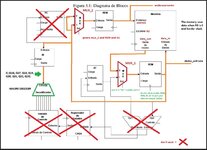
I will explain what I want.
I want to make an 8-bit data input via "dados_entrada" be put into the output Q : (Q16, Q17, Q18, Q19, Q20, Q21 Q22, Q23 ).

For that, this data inserted via "dados_entrada" must be saved in a random position informed by the "enderecamento", which is linked to the "address" of the memoria.

Finally, when the memory address is saved and, later, when this address is accessed again and the save value is placed in "data_out", I want this data to walk to the output Q. (see image)

Sem título.jpg


I'm working with the code from the first post now, that one has declared components
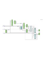
The RTL Viewer of my actual project is ->


0001.jpg


In this new code, I don't want the output of Q (Q16, Q17, ...), I want the output of the decoder O (O1, O2, O3, O4, O5, O6, O7, O8). So disregard the "IGNORE DECODER" in the image above.
 

Attachments

  • RTL_VIEWER_Projeto_Neander.pdf
    84.4 KB · Views: 94
Last edited by a moderator:

874611.jpg


See that no data comes out in the "data_out" of memory. It even seems that it is not being used even with all the pulses configured correctly.
I tested this same "memory_16x8" alone in ModelSim 10.3 and it worked perfectly.

I assume the components are not being used, but I don't know, I'm new to VHDL.
--- Updated ---

I will leave my code here complete here in case any friend knows where this error is and can tell me.
'Cause I can't find it
 

Attachments

  • Projeto_Neander_2.rar
    4.1 MB · Views: 100
Last edited:

Sorry, but what a mess. It sounds like you are simply trying to read and write from a memory, right? And you've turned this simple task into a tangled nightmare.

Regardless: Look at your simulation. dados_entrada is your input, right? dados_entrada is xxxxxxxx.

GARBAGE IN, GARBAGE OUT.
 

Sorry, but what a mess. It sounds like you are simply trying to read and write from a memory, right? And you've turned this simple task into a tangled nightmare.

Regardless: Look at your simulation. dados_entrada is your input, right? dados_entrada is xxxxxxxx.

GARBAGE IN, GARBAGE OUT.
Yes bro, like I said, I'm a beginner and I don't master of the language.
Would you help me ?

Yes, dados_entrada is my input which was declared in top level entity, it connects to the data_in of the memory
 
Last edited:

Hi,

I have not followed the thread to the end but I found a clue in post #5.

You have mixed up port types in your port declarations. For every signal, the port types in both components and top-level entities should be same.

If the port type was input in the lower level file, then it should be input in top-level file. If it was output in lower level file, it should be output in top-level file.

What you needed to have done when you had the port mismatch error - "a port of type IN cannot be assigned to a port of type OUT" - was to change the type of the affected port(s) in your top-level port declaration to the type corresponding type in your lower level files.

I hope this helps.
 
Yes bro, like I said, I'm a beginner and I don't master of the language.
Would you help me ?

Yes, dados_entrada is my input which was declared in top level entity, it connects to the data_in of the memory
And as I said, you've got garbage on dados_entrada. How do you expect to read anything out of memory when you're writing garbage to it?

As I mentioned early on, there may be something wrong with your testbench, and that appears to be the case here, since dados_entrada is undriven.
 
There isn't a testbench in their rar file, nor does the top level code Projeto_Neardor.vhd elaborate correctly (Vivado won't elaborate the top level). There are missing ports on one of the instantiations.

I've looked over the code in the rar and it is a mess.
  • using when statements to generate registers, instead of a process.
  • buffer and inout ports in the design.
  • names like C_L_O_C_K, C_L_K, CLK, and CLOCK? This design doesn't appear to be a multi-clock design, so why rename the clocks?
  • Poor port names that are meaningless.
Given buffer/input is used the original problem with OUT was probably caused by "reading" an OUT port in the architecture, because they didn't compile with 2008. The standard method (when you can't use 2008) is to use an internal signal, e.g. my_output_int and then assign it to the OUT port my_output <= my_output_int;

You need to go through some VHDL tutorials to learn how to write proper VHDL and then start over with this project.
https://www.nandland.com/vhdl/tutorials/tutorial-introduction-to-vhdl-for-beginners.html
http://asic-world.com/examples/vhdl/index.html
 

Would anyone know why when accessing position 0001 the data "00000001" is correctly inserted in the output, but when accessing position 0010 the data in output is incorrect?


1647613360682.png


Here's how the memory was initialized:


1647613487098.png


The memory code remains the same as I posted above, the difference is that I initialized the memory with the values in the image above;
 
Last edited:

What? WHAT??

“The memory code remains the same as I posted above, the difference is that I initialized the memory with the values in the image above“—what does that mean? It’s the same but different?

And maybe identify what those signals in your display are.
 
I isolated the memory circuit and found that it is generating the outputs correctly.
I verified that the problem is in my MUX, where the generated outputs are incorrect


1647620135000.png


The memory output connects directly to the MUX inputs A0, B0, ..., ..., A3, B3

I'm inserting 8 bits and it's returning me only the last 4 bits
But as my values are in the format "0000XXXX", where the "X" are values 1 or 0, I think I have no problem with that.
The problem seems to be in the inner circuit.
I will analyze the output for each value in the input.


1647620638454.png


the outputs are coming out inverted too
"00000001" = "10000000"
but this not is main problem
--- Updated ---

how do i connect port A0 to A4 without getting errors?


Code:
P3: entity work.mux_1
    port map(
        -- SIGNALS
        A0 => t1,
        B0 => t2,
        A1 => t3,
        B1 => t4,
        A2 => t5,
        B2 => t6,
        A3 => t7,
        B3 => t8,
          
        A4 => t9,
        B4 => t10,
        A5 => t11,
        B5 => t12,
        A6 => t13,
        B6 => t14,
        A7 => t15,
        B7 => t16,


I've tried several different ways and it keeps giving me an error.
 
Last edited:

I already identified the error, the circuit was correct! The problem was that I had to add the outputs like this:


Code:
P3: entity work.mux_1
    port map(
        -- SIGNALS
          --porta 0
        A7 => t1,
        A6 => t2,
        A5 => t3,
        A4 => t4,
        A3 => t5,
        A2 => t6,
        A1 => t7,
        A0 => t8,
          --porta 1
        B7 => t9,
        B6 => t10,
        B5 => t11,
        B4 => t12,
        B3 => t13,
        B2 => t14,
        B1 => t15,
        B0 => t16
     );
 

Status
Not open for further replies.

Part and Inventory Search

Welcome to EDABoard.com

Sponsor

Back
Top