Continue to Site

Welcome to EDAboard.com

Welcome to our site! EDAboard.com is an international Electronics Discussion Forum focused on EDA software, circuits, schematics, books, theory, papers, asic, pld, 8051, DSP, Network, RF, Analog Design, PCB, Service Manuals... and a whole lot more! To participate you need to register. Registration is free. Click here to register now.

Antenna matching network

Status
Not open for further replies.

ctzof

Full Member level 3
Full Member level 3
Joined
Mar 1, 2012
Messages
157
Helped
12
Reputation
24
Reaction score
11
Trophy points
1,298
Location
Munich
Visit site
Activity points
2,516
Hello,

I am more or less new to this. I want to insert two antennas to TI's WL1801MOD. The first antenna is a chip antenna ANT016008LCD2442MA1 and the other one an external antenna connected to a 50 ohm cable through a connector. What should I have to consider in this design. Just design 50 ohm impedance line from the chip to the antennas is enough or I have also design a matching network. Does the length of the line plays any particular role when designing a matching network. I'll also have to meet the FCC requirements for WLAN. You can take an idea of what I want to do by looking in the attached picture. I don't know if the circuit is correct I've more or less copied other designs from evaluation boards. Can anyone help me with this? Thanks.

- - - Updated - - -

This is the picture Unbenannt.jpg
 

One or two antennas connected at the same time will alter impedance seen by transceiver and impedance seen by internal antenna.
Matching network or coax cable will act as stub-matching for the other antenna.
A common way is to integrate a switch in CON2, switching to internal antenna only when no external antenna connector is inserted.
Then match for 50 Ohm at CON2 against transceiver and match internal antenna to 50 Ohm at the point it connects to CON2.
 

Unbenannt1.pngUnbenannt2.png
One or two antennas connected at the same time will alter impedance seen by transceiver and impedance seen by internal antenna.
Matching network or coax cable will act as stub-matching for the other antenna.
A common way is to integrate a switch in CON2, switching to internal antenna only when no external antenna connector is inserted.
Then match for 50 Ohm at CON2 against transceiver and match internal antenna to 50 Ohm at the point it connects to CON2.

Thanks for the answer. I suppose by internal antenna you mean the chip antenna? In the following pictures they use the same topology an external antenna and a chip antenna with exactly the same components but they use different circuits for antenna matching. Additionally they use different components for chip antenna matching than the ones proposed in the datasheet (**broken link removed**). And there is no switch between them. So I want to use the same topology but I don't know what circuit to use for antenna matching.
 

Yes, chip antenna is an internal antenna that is supposed to be mounted on a PCB.

Selecting int/ext antenna, compare how it is solved in 3/4G broadband modems which have coaxial connector for external antenna as alternative to internal antenna.
Who ever "they are", they are doing it wrong. Depending on application, do not think a such solution will be accepted by FCC either. They want to measure total TX power in a connector, but now will big part of total power be either reflected back to radio-chip or lost in internal antenna.
It will probably still work, but with somewhat reduced performance, depending on where TX and RX power is lost.

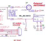
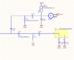
Thanks again. Just to determinate something we don't want to use both antennas at the same time. One of them is going to be used each time. So the correct schematic can be seen in the following picture. We want each time to discard ether C166 or C167 so the two antennas are going to be totally isolated. So which is the best solution for me. I have probably try to follow what the manufacturer of the chip antenna suggests in the datasheet. Do I have also try to include a matching network for the external antenna or a 50 ohm line is ok? What I am thinking is that they put additional components and they do the matching with a network analyzer later so the more components they include in the matching network the easier is to match the antenna with a network analyzer. Cause for example chip antenna manufacturer doesn't have this C165 capacitor in the datasheet, I think they put it in the layout so they have later the ability to alter its value with VNA to produce the matching. Unbenannt4.png
 

Switching antenna by selecting either C166/167 is an variant that is good enough for impedance matching.
There are then a T network adjusting impedance at CON2, and also a T network for internal antenna. Match for 50 Ohm at external connector.
There is no need for 50 Ohm match at chip antenna or transceiver. Conjugate match is enough.

Sorry but I didn't understand exactly what you mean. I insert this T network for external antenna but is it necessary? In evaluation boards the don't use any matching network they just directly connect the external antenna with 50 ohm line. For the internal antenna I have to follow the matching network suggested by the manufacturer in the datasheet?
 

You already have a T network in the schematic, C166,L5, C164. No more components are needed.
Matching CON2 depends how much you want to optimize. Connect VNA to CON2 and measure. Expect something between 30-70 Ohm. Is that ok, then is no matching needed and component pads can be removed, if not needed for DC-decoupling.
Else is it relative cheap to leave space for matching, just in case and as it later maybe shows that matching really was needed, which then cost a new PCB layout if unneeded pads have been removed.
If it is a lightweight headset where every extra hour from battery is an big advantage and max RF coverage distance is needed, can a proper precision TIS and TRP-matching be of high value. If it is a cheap toy-product, remove every component that not is absolutely needed to get some function at all. It is your decision.
 
  • Like
Reactions: ctzof

    ctzof

    Points: 2
    Helpful Answer Positive Rating
You already have a T network in the schematic, C166,L5, C164. No more components are needed.
Matching CON2 depends how much you want to optimize. Connect VNA to CON2 and measure. Expect something between 30-70 Ohm. Is that ok, then is no matching needed and component pads can be removed, if not needed for DC-decoupling.
Else is it relative cheap to leave space for matching, just in case and as it later maybe shows that matching really was needed, which then cost a new PCB layout if unneeded pads have been removed.
If it is a lightweight headset where every extra hour from battery is an big advantage and max RF coverage distance is needed, can a proper precision TIS and TRP-matching be of high value. If it is a cheap toy-product, remove every component that not is absolutely needed to get some function at all. It is your decision.

OK thanks a lot!! Your answer is very helpful. The bad thing is that we don't have a VNA, so it would be difficult to retune a matching network at the end. And what happens with components that are in series in this matching network if they are not needed I replace them with 50 ohm resistance? As for the chip antenna your pinion is to follow the matching network of in the datasheet right? Cause in evaluation boards they also added this C165 capacitor.
 

Verify and re-tune is just adjusting existing component values. It is common that it is done for final product revision as even minor track adjustment or things such as cover and battery location may have changed impedances a bit compared to initial prototype.
Not needed serial components are replaced with 0 Ohm resistors.
Datasheet or not, leaving space for a T network is a good idea. Actual values for chip-antenna tuning in evaluation board are as best correct values in that situation.
Even if you follow existing layout to 100%, and use exactly the same type of cover and have a similar ground-plane will probably PCB dielectric constant be different, and then is a retuning needed for max performance.

Can you suggest a starting matching network for the external antenna cause I don't know if the one I am using right now is good. I want also to include C157 as an esd suppressor. I want to use external antenna for the the standard ISM band 2.442 GHz (BW=42MHz).
 

Use existing values as a start. They are probably better then any guess I am able to do. In worst case is coverage a bit short but it will work good enough to verify that it is alive.
With some luck are you satisfied with its wireless functionality as it is.
 

Use existing values as a start. They are probably better then any guess I am able to do. In worst case is coverage a bit short but it will work good enough to verify that it is alive.
With some luck are you satisfied with its wireless functionality as it is.

OK a last question.....I want a simple T network for matching, so should I remove C163 to construct this T network or not?
 

More component places gives better possibilities to implement a good network. If it not causes other problems, leave it as it is.
 

Are you sure on the original schematic, both antennas and networks are actually supposed to be populated at the same time? It would make sense if you only populated one at a time. But connecting two antennas to one port at the same time doesn't make any sense.
 

Are you sure on the original schematic, both antennas and networks are actually supposed to be populated at the same time? It would make sense if you only populated one at a time. But connecting two antennas to one port at the same time doesn't make any sense.

I know...I explained in a previous post that we are going to use one antenna at a time. We want each time to discard ether C166 or C167 so the two antennas are going to be totally isolated and one of them is going to be used each time so either C167 or C166 is going to be unmounted.
 

More component places gives better possibilities to implement a good network. If it not causes other problems, leave it as it is.

We want to use the external antenna at 2.44 GHz but after some simulations I've made this network doesn't behave good at this frequency band. The thing is that I am supposed to design the structure for a matching network for a circuits that already supposed to have 50 ohms output and input impedance (IC and antenna) and I don't know what to put cause simulators for example don't give any result if impedances are the same simply because you don't need any matching. Do you have anything to propose?
 

As you say, no matching network needed.

Particularly I don't understand the reasoning behind a highpass LC network. A low-pass could be at least designed as a harmonic filter with 50 ohm in- and output impedance.
 

As you say, no matching network needed.

Particularly I don't understand the reasoning behind a highpass LC network. A low-pass could be at least designed as a harmonic filter with 50 ohm in- and output impedance.

This was not designed by me I don't know the reason why he put this matching structure in external antenna. My question is what structure I have to put at the beginning so I can later calibrate those components with VNA. For sure under the given specifications we don't need any matching network but because probably antenna is going to be unmatched in the final board I want to have space and components that I will later be able to change-calibrate with VNA to be matched at 50 ohms. All I want is a good starting point for this structure. As I wrote external antenna is going to work at 2.44 GHz (BW=40 MHz). Should I start then with a harmonic low or highpass filter cause its very difficult to design bandpass filter at this frequency with lumped components. I want to have at the end something similar to PI or T matching network structure.
 

Status
Not open for further replies.

Part and Inventory Search

Welcome to EDABoard.com

Sponsor

Back
Top