rxnr
Newbie
Hello.
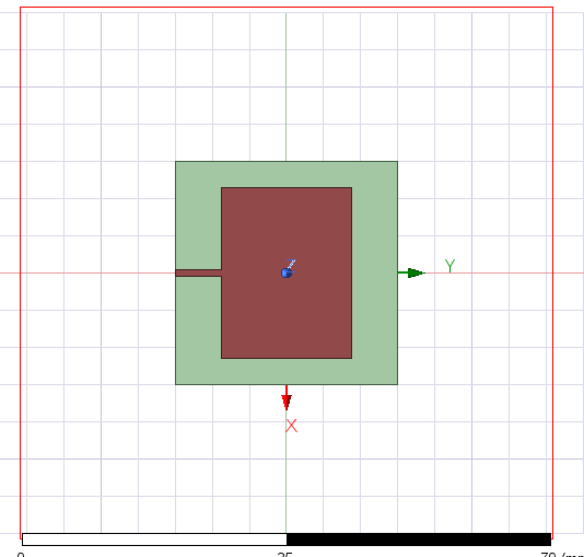
I am currently trying to parameterize the feedline position on my rectangular microstrip patch antenna on HFSS. For reference, here is my design.

I am trying to offset the location of the feedline along the x-axis to optimize the performance. For this, I am trying the parameterize options in HFSS. I have tried setting the range of the x-coordinate from -8 to 8 with a step of 1. The nominal value, ie, location of feedline in the image is at -0.5.
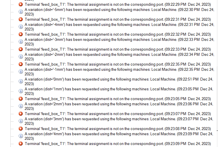
And on validation and simulation, I only get results for -1, 0.5 and 1 while the others have this particular error.

As you can see, only -1, 0 and 1 are simulated. How can I rectify this error?
Thank you for taking the time to read so far.
Hoping for help!
I am currently trying to parameterize the feedline position on my rectangular microstrip patch antenna on HFSS. For reference, here is my design.
I am trying to offset the location of the feedline along the x-axis to optimize the performance. For this, I am trying the parameterize options in HFSS. I have tried setting the range of the x-coordinate from -8 to 8 with a step of 1. The nominal value, ie, location of feedline in the image is at -0.5.
And on validation and simulation, I only get results for -1, 0.5 and 1 while the others have this particular error.
As you can see, only -1, 0 and 1 are simulated. How can I rectify this error?
Thank you for taking the time to read so far.
Hoping for help!