Continue to Site

Welcome to EDAboard.com

Welcome to our site! EDAboard.com is an international Electronics Discussion Forum focused on EDA software, circuits, schematics, books, theory, papers, asic, pld, 8051, DSP, Network, RF, Analog Design, PCB, Service Manuals... and a whole lot more! To participate you need to register. Registration is free. Click here to register now.

analog pcb using allegro16.3

Status
Not open for further replies.

danismith

Member level 2
Joined
May 29, 2013
Messages
47
Helped
0
Reputation
0
Reaction score
0
Trophy points
1,286
Activity points
1,584
hai friends,
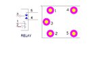
Am just trying to route an Analog board,in that can a track pass between 2 pins of a transformer? smps routing.JPG

this type of routing is wright or wrong ?
 

Can we presume that track widths and minimum distance design rules have been choosen according to electrical requirements (voltage and current)? Then it should be O.K.

Reviewing some layout details, I have doubts about a plausible selection of trace widths. But that's just a guess that can't be checked without a schematic.
 

hai,
Am not sure about this contraint manager culture,but i can give u the schematic,

- - - Updated - - -

smps jpeg.JPG see this and give your command,if any mistake inform me.


thank u

- - - Updated - - -

if this is not clear send ur email address i'll send u in pdf format

- - - Updated - - -

hai,
can u tell me, how to assign the values in constraint manager.one of my friend said ,to change the value of a track , right click->change track width.
but when i gave the board for fabrication they asked me to change the line spacing.

so plz help me?
 

The schematic confirms by worst suspicion. The circuit seems to be intended to work with mains input voltage and safe insulation.

You have < 0.5 mm clearance where you need 3 to 6 mm, depending on the applied safety standard, and very thin tracks for currents of several amperes. Wrong pin assignment of some components (MOSFET, schottky rectifier) is a minor problem in this regard.

Starting over!
- review requirements for PCB track width and clearance for different current and voltage levels
- consider double/reinforced insulation between mains and low voltage circuits
- define net classes and design rules according to this requirements
- double check the pin assignment of self defined components
- think about a placement topology that allows to keep the clearance between primary and secondary circuit and sufficient track widths (the transformer e.g. has to be rotated), the mains input connected must be moved to the left side
- study the layout of commercial power supplies or reference designs from semiconductor manufacturers. They can be expected to keep to safety rules (with the exception of some cheap chinese devices).
 

hi,
now i have understood some ,that
1. i must route the ground lines separately
2.should divide the design as primary,secondary,ac, dc lines

see this attached image and pass ur commands,
am wait for my revaluation results.SMPS UPDATE1.JPG
 

Looks like it can achieve the required clearance between primary and secondary side.

It might be reasonable to place the switch transistor Q1 nearer to the transformer.
 

hi,
thank u for ur instruction,one more correction can u just verify this foot print( package number),
relay.JPG

i saw many diagrams it is confusing can help me?
 

Attachments

  • relay.JPG
    relay.JPG
    28.8 KB · Views: 94
  • relay.JPG
    relay.JPG
    28.8 KB · Views: 98

The pin positions of this popular relays type are clearly described in manufacturer datasheets, e.g. https://www.omron.com/ecb/products/pdf/en-g5le.pdf

Please pay attention to bottom view/top view indication

Presuming you are showing the PCB form editor view (top view), N.O. and N.C. contact have to be exchanged.
 

This is a SMPS design and as such requires careful layout otherwise it will be extremely noisy and may not work.
I cant read what the controller is, but I would look for the data sheet and any layout guides for such device. I would also look up information on SMPS layout as it is rather specialised, and bad layouts give SMPS supplies a bad and unjustified name due to the EMC they can generate.
 

Status
Not open for further replies.

Part and Inventory Search

Welcome to EDABoard.com

Sponsor

Back
Top