maxporter
Junior Member level 2
Hey all,
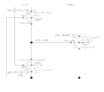
I have a simple max voltage selector (2x 3V3 PMOS, alternative design is 4x stacked PMOS). Inputs are VDD (fixed voltage reference) and VSEL (more or less digital waveform). The output (which is always the highest voltage) goes to the gate of a fairly big PMOS. In principle this works fine, unless VSEL is changing rapidly and the high state is equal to VDD. When VSEL is ramping up from 0 -> VDD, eventually all PMOS goes off, the gate connection becomes high ohmic, causing a large initial spike (>4V5) which degrades slowly back to 3V3. Since this potentially could damage the gate, is there a way to avoid this? Or perhaps provide some kind of discharge path (preferably without wasting static current).
Thnx in advance.

