Welcome to our site! EDAboard.com is an international Electronics Discussion Forum focused on EDA software, circuits, schematics, books, theory, papers, asic, pld, 8051, DSP, Network, RF, Analog Design, PCB, Service Manuals... and a whole lot more! To participate you need to register. Registration is free. Click here to register now.
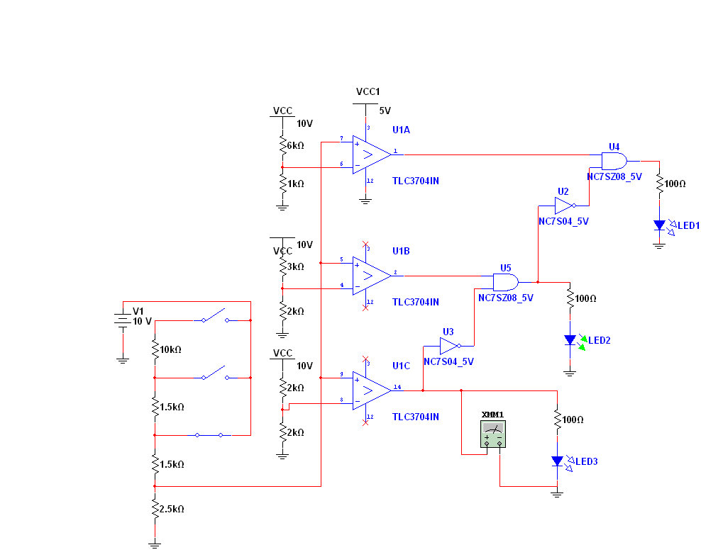
When LED3 is on you should see LED1 and LED2 OFF, since the inverter U5A will apply a low state on the last AND of both of them. The problem could be that U1A is not able to sink the 5mA current. The difference with respect to U6B is that U1A has one input to HIGH and the other one to LOW, U6B instead has both inputs to LOW. You can try to measure the currents flowing into the LEDs and into the gates.
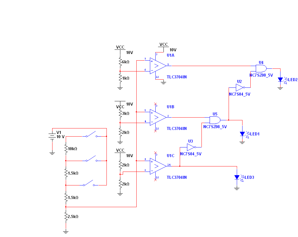
Draw the parts on the schematic closer together then it can be zoomed so we can read the tiny numbers on it.
I managed to see the schematic by downloading the DOC file (why use a DOC file for a schematic?) and zooming in on parts of it.
The parts are so far apart that the schematic is the size of my neighbourhood.
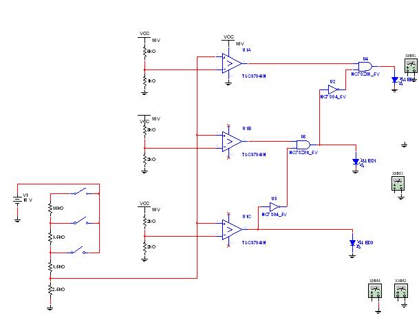
I see that the +8.8V output high of the LM358 opamps will destroy the inputs of the old TTL logic ICs.
Your new circuit will not work because:
1) The output high of the TLC3704 will go to +10V but the max allowed input voltage of the AND gate and logic inverter are their supply voltage which is not shown. The max allowed supply is only 6V. Make the supply for all 3 ICs 5V.
2) Nothing limits the current in the LEDs so they might burn out.
3) The LEDs limit the voltage so that the inputs of the logic inverters will never be a logic high.
No it is not.
Figure 13 in the datasheet of the TLC3704 shows that with a 5V supply and an 18mA load from a 2.0V red LED in series with the 100 ohm resistor, the typical output voltage will be +3.7V. It might be a little lower and it might be a little higher.
The minimum input high voltage of an NC7SZ08 is +3.7V so the output from the TLC3704 might be too low and not work.
If you reduce the load on the output of the bottom TLC3704 and on the middle AND gate with a transistor to drive the LEDs then every circuit that is made will work perfectly.
Finally, always have positive hysteresis around comparators. See app notes on the National, Analog Devices, or T.I.
websites. Otherwise, with slow input waveforms, they willl oscillate.
This site uses cookies to help personalise content, tailor your experience and to keep you logged in if you register.
By continuing to use this site, you are consenting to our use of cookies.