Continue to Site

Welcome to EDAboard.com

Welcome to our site! EDAboard.com is an international Electronics Discussion Forum focused on EDA software, circuits, schematics, books, theory, papers, asic, pld, 8051, DSP, Network, RF, Analog Design, PCB, Service Manuals... and a whole lot more! To participate you need to register. Registration is free. Click here to register now.

Altium mixed simulation - MOSFET not simulated correctly?

Status
Not open for further replies.

TnF

Junior Member level 3
Joined
Mar 1, 2015
Messages
31
Helped
1
Reputation
2
Reaction score
1
Trophy points
8
Visit site
Activity points
350
Hello guys. I'm new to electronic design, but i just got into simulation. So to keep the question short basically i localized my problem to a specific component i use in Altium designer. It's an IRL2203N mosfet. Because i did try several things with no avail i just made a simple schematic and the problem now is very clear. I get a 2.35V drop across VDS. VGS is 5V, same as my VDS. My load is connected to the source (even though ideally you want to connect it in the drain - i'll test that way in a bit if it makes any difference). I know that i will have a small voltage drop across but look at the datasheet MAX 10mohm at VGS=4.5V. I'm not even doing any high frequency switching. Signal is a 4ms pulsewidth, >100hz pulse. Altium uses the following Spice model:
Code:
**************************************
*      Model Generated by MODPEX     *
*Copyright(c) Symmetry Design Systems*
*         All Rights Reserved        *
*    UNPUBLISHED LICENSED SOFTWARE   *
*   Contains Proprietary Information *
*      Which is The Property of      *
*     SYMMETRY OR ITS LICENSORS      *
*Commercial Use or Resale Restricted *
*   by Symmetry License Agreement    *
**************************************
* Model generated on Sep 27, 01
* MODEL FORMAT: SPICE3
* Symmetry POWER MOS Model (Version 1.0)
* External Node Designations
* Node 1 -> Drain
* Node 2 -> Gate
* Node 3 -> Source
.SUBCKT irl2203n 1 2 3
M1 9 7 8 8 MM L=100u W=100u
.MODEL MM NMOS (LEVEL=1 IS=1e-32
+VTO=2.36103 LAMBDA=0.0325968 KP=204.753
+CGSO=3.1e-05 CGDO=1e-11)
RS 8 3 0.00427452
D1 3 1 MD
.MODEL MD D (IS=8.56401e-11 RS=0.00355838 N=1.14431 BV=30
+IBV=0.00025 EG=1 XTI=1 TT=0
+CJO=4e-09 VJ=1.16989 M=0.419864 FC=0.5)
RDS 3 1 1e+06
RD 9 1 0.0001
RG 2 7 6
D2 4 5 MD1
* Default values used in MD1:
*   RS=0 EG=1.11 XTI=3.0 TT=0
*   BV=infinite IBV=1mA
.MODEL MD1 D (IS=1e-32 N=50
+CJO=1.87864e-09 VJ=1.71885 M=0.867625 FC=1e-08)
D3 0 5 MD2
* Default values used in MD2:
*   EG=1.11 XTI=3.0 TT=0 CJO=0
*   BV=infinite IBV=1mA
.MODEL MD2 D (IS=1e-10 N=0.4 RS=3e-06)
RL 5 10 1
FI2 7 9 VFI2 -1
VFI2 4 0 0
EV16 10 0 9 7 1
CAP 11 10 3.38961e-09
FI1 7 9 VFI1 -1
VFI1 11 6 0
RCAP 6 10 1
D4 0 6 MD3
* Default values used in MD3:
*   EG=1.11 XTI=3.0 TT=0 CJO=0
*   RS=0 BV=infinite IBV=1mA
.MODEL MD3 D (IS=1e-10 N=0.4)
.ENDS irl2203n

What is going on? Is it because of the model file?

Kind regards,
Ken
 

I get a 2.35V drop across VDS. VGS is 5V, same as my VDS.

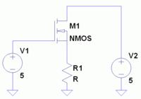
Are you talking about a source follower circuit like below? Vds can't drop below Vgs threshold in this case. Everything normal operation.

Increase V1 above V2 to turn the MOSFET fully on.


Are you talking about a source follower circuit like below? Vds can't drop below Vgs threshold in this case. Everything normal operation.

Increase V1 above V2 to turn the MOSFET fully on.


Yes like that. VDS is above or equal VGS. Is there is a specific case that the MOSFET will not fully activate? This is a logic level N-channel mosfet which has a VGS threshold of 1V, and at VGS=4.5V can pass 48A which less than 10mohm parasitic resistance. Even looking at the datasheet: **broken link removed** Fig.1 p.3 at VDS=5V and VGS=4.5V, IDS is >100A.

However here is what i'm doing in Altium (please click to see full-res image):

Version 1 (load connected at source):


Version 2 (load connected at drain):


In Version 2, it doesn't look to have any losses. So what i'm doing wrong?


I think you are simply missing the meaning of Kirchhoff's voltage law. https://en.wikipedia.org/wiki/Kirchhoff's_circuit_laws#Kirchhoff.27s_voltage_law_.28KVL.29

If you apply 5V pulse voltage between gate and circuit ground, the voltage between source and ground will be always smaller by the gate voltage amount required for the respective load current, at least gate threshold voltage. That's what we see in your simulation waveform.

Yes i understand that. That's why i said there is a 2.35V drop as 5V - 2.65V (show in the "netload_2" part of the graph in Version 1). But it shouldn't be anywhere near that much. As the gate is raised at a higher potential difference (relative to source) the mosfet initially starts to conduct with a high internal resistance which lowers as the gate's potential difference is increased further. From the datasheet we know that the internal resistance will be less than 10mohms. So we have a total resistance of 380.01ohms in the D-S-Gnd path. At at 5V the current flowing is 13.158mah. So the voltage drop across D-S should be 0.1318mV..not 2.35V! Sorry i know i'm missing something simple here but i am kinda lost :/

- - - Updated - - -

Basically after i did some experimentation i do i understand what is my problem. Basically in order for the mosfet to fully saturate VGS must be higher than VDS by the threshold voltage. And now my question, how do i switch a high power 5V regulated supply with an arbitrary 5V signal? If i want to use the mosfet i need to amplify in some way my signal right? But i though the whole point was using this transistor to "amplify" my signal :/
 

So went and researched a bit more of the topic and basically the whole effect is because i have the load connected to the source side. But why this happens? I thought since the load is in the same current path there shouldn't have any effect on the mosfet. However it seems that if the load is connected on the Vdd side it has a voltage drop as soon the mosfet is activated so that vds<vgs and it saturates fully. On the other hand if the load is connected on the source side this voltage drop somehow affects the saturation of the mosfet..can someone please explain? Thanks
 

Status
Not open for further replies.

Part and Inventory Search

Welcome to EDABoard.com

Sponsor

Back
Top