Continue to Site

Welcome to EDAboard.com

Welcome to our site! EDAboard.com is an international Electronics Discussion Forum focused on EDA software, circuits, schematics, books, theory, papers, asic, pld, 8051, DSP, Network, RF, Analog Design, PCB, Service Manuals... and a whole lot more! To participate you need to register. Registration is free. Click here to register now.

ADS Momentum: Determining the Inductance of a Planar Coil

Status
Not open for further replies.

banenane

Newbie level 3
Newbie level 3
Joined
Sep 2, 2014
Messages
4
Helped
0
Reputation
0
Reaction score
0
Trophy points
1
Visit site
Activity points
39
Hello!

I want to simulate and compare the inductance/resistance of different planar coils in ADS 2014 Momentum. To familiarize with the program, I rebuilt a coil with known parameters in the layout window (N=30, 4mm x 4mm) using MRIND. The substrate is: conductor(copper) -- 500um FR4 -- AIR. After the simulation from 8MHz to 14Mhz, the results using the "S2port_Spiral" template were significantly different to the known values (L=2.4uH instead of 5.3uH, R=350Ohms should be about max 50).

The only warning I get is: "Port 1/2 does not have an explicit reference pin,
S-parameters may become unphysical at higher frequencies." So I added a conducting cover plane to my substrate. The problem is that this ground plane has to be in the proximity of the coil (otherwise I get another warning/momentum tries to move the plane by itself) and of course that changes the behavior of the coil.

I'm new to ADS and somewhat to EM Simulations, so I don't know what I'm doing wrong at the moment, but I'm sure that I do :)
 

Where is your GND ?? If there isn't any GND, you should assign a GND like planar layer to each Port as a reference terminal in Substrate editor.Positive terminal will touch to "Conductor2", Negative terminal will touch to "Conductor" layer in your case.Therefore Momentum is saying "Port 1/2 does not have an explicit reference pin".
 

Where is your GND ?? If there isn't any GND, you should assign a GND like planar layer to each Port as a reference terminal in Substrate editor.Positive terminal will touch to "Conductor2", Negative terminal will touch to "Conductor" layer in your case.Therefore Momentum is saying "Port 1/2 does not have an explicit reference pin".

Wen I introduce a groundplane (PEC cover) to my substrate to connect my reference pins to, I encouter following problems:

1. I cannot specify that the groundplane is infinitely far away from my device.
2. Manually entering a large distance (e.g. 1000m) results in a error message during the simulation.
("Failed to converge for high-end frequencies (>= 9.8e-005 GHz).")

3. Putting the ground plane near the object (10m, 1m, 10cm) changes the simulation results.

Is there a possibility to set the groundplane infinitely far away?
 

coil with known parameters in the layout window (N=30, 4mm x 4mm) using MRIND. The substrate is: conductor(copper) -- 500um FR4 -- AIR. After the simulation from 8MHz to 14Mhz, the results using the "S2port_Spiral" template were significantly different to the known values (L=2.4uH instead of 5.3uH, R=350Ohms should be about max 50).

With the given parameters and 4mm outer diameter, the inductance of ~2.4nH looks correct. I get 2.5nH using this online calculator
http://www-smirc.stanford.edu/spiralCalc.html

The only warning I get is: "Port 1/2 does not have an explicit reference pin,
S-parameters may become unphysical at higher frequencies." So I added a conducting cover plane to my substrate.

No, there is a better way. You can get away without an infinite ground if you group pins P1 and P2 into one differential port, where P1 is the plus terminal and P2 is the minus terminal. To do this, open the port editor and move P2 to the minus symbol of P1 using drag & drop. Now you have one differential port between P1 and P2, which works fine with your substrate from post #1. No infinite ground plane reqired in this case.
 
Last edited:
Is there a possibility to set the groundplane infinitely far away?

No..Every RF current must return back its source.Therefore a port has 2 pins.While first pin excites the circuit the other is used return path.
It's a electrical circuit, if you make GND open circuit, the circuit won't work, it's clear.That is similar to this case...
 

With the given parameters and 4mm outer diameter, the inductance of ~2.4nH looks correct. I get 2.5nH using this online calculator
http://www-smirc.stanford.edu/spiralCalc.html

Great, thanks! Apparently my information concerning the 5 uH were wrong...

No, there is a better way. You can get away without an infinite ground if you group pins P1 and P2 into one differential port, where P1 is the plus terminal and P2 is the minus terminal. To do this, open the port editor and move P2 to the minus symbol of P1 using drag & drop. Now you have one differential port between P1 and P2, which works fine with your substrate from post #1. No infinite ground plane reqired in this case.

Interesting idea, but it didn't work out for me. Converting the S11 to Y and then to L yielded questionable results (Something in the range of pH).

No..Every RF current must return back its source.Therefore a port has 2 pins.While first pin excites the circuit the other is used return path.
It's a electrical circuit, if you make GND open circuit, the circuit won't work, it's clear.That is similar to this case...

There were reference pins marked as GND in the port menu. I did not want to add a conducting layer to my substrate because it interferes with the DUT. I wanted to simulate in a kind of free space condition, like when simulating an antenna in CST.
 

In my previous design, I used GND layer, that is to isolate different signals.
I believe good design should have GND, and the gap for GND should be simulated.
 

Interesting idea, but it didn't work out for me. Converting the S11 to Y and then to L yielded questionable results (Something in the range of pH).

Believe me, I am application expert for inductor EM simulations for many years.
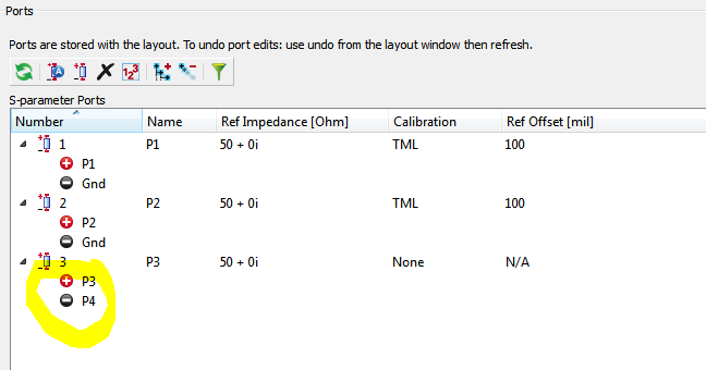
You need to group the pins into a differential port, and then it will look in the port editor as port 3 shown here (with P3/P4):
differentialport.png

In the picture, there are more ports because this is not an inductor. In your case, you will have a single port with P1/P2.

You might have made some mistake with the math converting from S11 to the inductor parameters.

There were reference pins marked as GND in the port menu. I did not want to add a conducting layer to my substrate because it interferes with the DUT. I wanted to simulate in a kind of free space condition, like when simulating an antenna in CST.

That's a valid approach, and your initial substrate definition is correct for that. The only requirement then is to group P1 and P2 into one differential port.

For other application, where we really have a conductor below (like substrate in Si RFIC) we prefer 2-port simulations.
https://muehlhaus.com/support/ads-application-notes/inductor-em-ports
But in your case, the 1-port simulation is fine.

- - - Updated - - -

No..Every RF current must return back its source.Therefore a port has 2 pins.While first pin excites the circuit the other is used return path.

This is correct, but it does not mean that we need an infinite ground. Momentum can use ports referenced to an infinite ground, or ports referenced to another pin ("differential ports"):

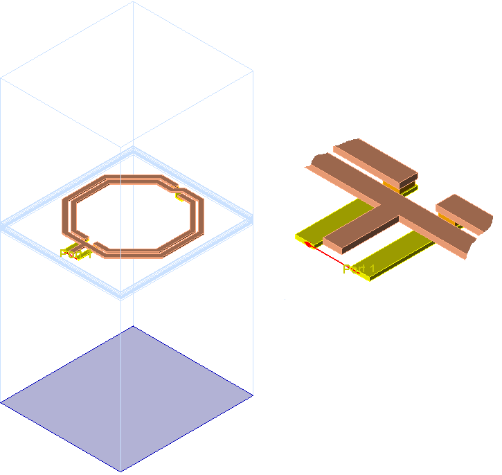
Port referenced to an infinite ground:
inductor_3D_2port.png


Port referenced to another pin (infinite ground NOT required)
inductor_3D_1port.png
 
  • Like
Reactions: vsnr and banenane

    banenane

    Points: 2
    Helpful Answer Positive Rating
    V

    Points: 2
    Helpful Answer Positive Rating

    vsnr

    Points: 2
    Helpful Answer Positive Rating
Thank you very much volker@muehlhaus! I have simulated some known inductors and could verify my simulations using the differential port setup. Also thanks for the link to your site, the tutorials are very informative!
 

Status
Not open for further replies.

Part and Inventory Search

Welcome to EDABoard.com

Sponsor

Back
Top