Continue to Site

Welcome to EDAboard.com

Welcome to our site! EDAboard.com is an international Electronics Discussion Forum focused on EDA software, circuits, schematics, books, theory, papers, asic, pld, 8051, DSP, Network, RF, Analog Design, PCB, Service Manuals... and a whole lot more! To participate you need to register. Registration is free. Click here to register now.

Adding material to the face of the substrate

Status
Not open for further replies.

Prospermin

Newbie level 1
Joined
Aug 13, 2015
Messages
1
Helped
0
Reputation
0
Reaction score
0
Trophy points
1
Location
Shillong
Activity points
8
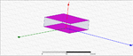
Hello, can anyone help me...? I want to design a new project. At the start of the project, I chose a box in which by default the material is vacuum. I want to design in which the two faces of the substrate in the z-axis to be copper but the spaces between the two faces to be vacuum.
 

Attachments

  • HFSS.png
    HFSS.png
    65.8 KB · Views: 90

If you consider your copper electrodes as perfect conductors (if you don't care about field penetration into the conductor or resisitive losses) you can simply assign perfect-E boundary condition to these faces.
 

Status
Not open for further replies.

Part and Inventory Search

Welcome to EDABoard.com

Sponsor

Back
Top