Continue to Site

Welcome to EDAboard.com

Welcome to our site! EDAboard.com is an international Electronics Discussion Forum focused on EDA software, circuits, schematics, books, theory, papers, asic, pld, 8051, DSP, Network, RF, Analog Design, PCB, Service Manuals... and a whole lot more! To participate you need to register. Registration is free. Click here to register now.

About return path of spiral inductor simulation

Status
Not open for further replies.

hhxuexia

Newbie level 6
Joined
Nov 1, 2009
Messages
11
Helped
0
Reputation
0
Reaction score
0
Trophy points
1,281
Activity points
1,365
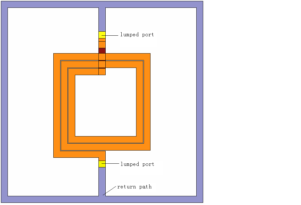
I'm simulating a spiral inductor with HFSS. Two terminals of the indutor lay on oposite sides. To form a complete loop for the current to flow, a return path is needed. As shown in the figure below, a square loop outside the inductor serves as return path, the square loop intersects with silicon substrate. But it was found, the simulated resulst is the unite of inductor and return path instead of inductor only. So, my question is, how to eliminate the effect of return path, or what kind of return path does not deteriorate simulation result? Thanks!

 
Last edited:

This is indeed a problem in modelling and measurement of N.5 turn inductors with feedlines on opposite sides. The inductor needs some return path - in simulation, in measurement and also in the circuit. In my opinion, the best solution is to include a return path that is simular (as much as possible) to the return path in the actual circuit.
 
Hi, volker_muehlhaus!
Thanks for your reply.

yes, the return path should be same with it in actual circuit. but in my actual circuit, the return path is very complicated, and there exist several return paths which contains capacitors, transistors, resistors and so on. I do not know how to demonstrate transistors in HFSS simulations?
By the way, in measurements, de-embeded(short, open, load, thru) operation can be used to get the exact characteristics of inductor. But in simulation, I find it's hard to do such operations in HFSS simulations. Have you ever do such operation in HFSS simulaitons?
Thanks.


This is indeed a problem in modelling and measurement of N.5 turn inductors with feedlines on opposite sides. The inductor needs some return path - in simulation, in measurement and also in the circuit. In my opinion, the best solution is to include a return path that is simular (as much as possible) to the return path in the actual circuit.
 

By the way, in measurements, de-embeded(short, open, load, thru) operation can be used to get the exact characteristics of inductor.

I have not found a way to remove the ground path issue by de-embedding.

But in simulation, I find it's hard to do such operations in HFSS simulations. Have you ever do such operation in HFSS simulaitons?

Over the past years, I have done hundreds of these inductor simulations and measured-calculated comparisons for various foundries. I use Sonnet, not HFSS.
 

Hi, volker_muehlhaus!
Thanks for your kindly reply!

have you ever meet return path probelms in sonnet ?
 
Last edited:

have you ever meet return path probelms in sonnet ?

Yes, this "problem" is indepent of the simulator. As I wrote above: There is no easy way to separate the inductor from the return path for these N.5 turn inductors. The best method that I know is to have a model that includes signal and return path, with return path layout in simulation similar to the return path in the circuit.
 

Yes, this "problem" is indepent of the simulator. As I wrote above: There is no easy way to separate the inductor from the return path for these N.5 turn inductors. The best method that I know is to have a model that includes signal and return path, with return path layout in simulation similar to the return path in the circuit.

Thanks a lot!
 

Status
Not open for further replies.

Part and Inventory Search

Welcome to EDABoard.com

Sponsor

Back
Top