bzr2915
Newbie level 6

Help! About PMOS Diode connection (current direction)

The figure above is a PMOS, when VL is higher than VR, there will be a current from VL to VR. It means that the diode turns on when it is forward-biased. On the other hand, when VR is higher than VL, the voltage of drain is higher than that of the substrate, so the drain-body junction starts to conduct.
Then my question is what is the diode direction? Base on the above statement it should be a bidirectional diode, right?

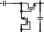
The figure above is voltage doubler and if it's a bidirectional thing how does it work?
PS: I notice if I change the voltage doubler to NMOS the output will become negetive instead of POMS positive. Why?
Thank you for your rely!

The figure above is a PMOS, when VL is higher than VR, there will be a current from VL to VR. It means that the diode turns on when it is forward-biased. On the other hand, when VR is higher than VL, the voltage of drain is higher than that of the substrate, so the drain-body junction starts to conduct.
Then my question is what is the diode direction? Base on the above statement it should be a bidirectional diode, right?

The figure above is voltage doubler and if it's a bidirectional thing how does it work?
PS: I notice if I change the voltage doubler to NMOS the output will become negetive instead of POMS positive. Why?
Thank you for your rely!
Last edited:

