Josephchiang
Member level 1

- Joined
- Oct 2, 2013
- Messages
- 38
- Helped
- 0
- Reputation
- 0
- Reaction score
- 0
- Trophy points
- 6
- Location
- Hsinchu, Taiwan, Taiwan
- Activity points
- 400
Hello everyone,
I am new to low drop-out voltage(LDO) regulator design
I have ever read a famous paper which tell me why PSRR get best reslut at low frequecny , 20db/dec degrading as frequency beyond error amplifier(EA) bandwidth, reach at worst case when frequency at the gain bandwidth product (GBW)of EA, 20db/dec increasing as frequecny over GBW, the PSRR curve was shown as belowing plot which was cutted from this paper

But I can't figure out why the PSR curve acts like that in my design
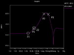
My simulation result was shown below. The circle and cross represent zero and pole,respectively

Compare simulation result with theoretical analysis result, it seem that there are additional zero Z2 exists at this curve (Z2 is very closed to P1)
The circuit block and detail schematic is shown below individually

The extra NMOS pass element with R2, C1 form a low pass filter. R2 and C1 was choosen to set the corner frequency of LPF at 17KHz. The dominate pole was set at the output of EA. The second pole was set at LOD output .
My analysis of the distribution of pole and zero of PSR: Z1 located at 3dB bandwidth of EA, P1 located at corner frequency of LPF, P2 located at GBW of EA and P3 locate at the LDO output pole frequecny
Beside Z2 , all the analysis is quite reasonable which also meet the simulation result
I have no ideal where did Z2 come from?
Base on the frequency of Z2, I try to infer that why Z2 exists
The possible reason of that is Z2 come from the corner frequency of bias circuit
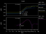
The PSR of BIAS circuit is shown below

Where V_source is connected to Mn14 and Mn15 , Vref is connected to Mn17, Vldo is connected to Mn18.
Please correct me if I'm wrong
Any help will be greatly appreciated
I am new to low drop-out voltage(LDO) regulator design
I have ever read a famous paper which tell me why PSRR get best reslut at low frequecny , 20db/dec degrading as frequency beyond error amplifier(EA) bandwidth, reach at worst case when frequency at the gain bandwidth product (GBW)of EA, 20db/dec increasing as frequecny over GBW, the PSRR curve was shown as belowing plot which was cutted from this paper

But I can't figure out why the PSR curve acts like that in my design
My simulation result was shown below. The circle and cross represent zero and pole,respectively

Compare simulation result with theoretical analysis result, it seem that there are additional zero Z2 exists at this curve (Z2 is very closed to P1)
The circuit block and detail schematic is shown below individually

The extra NMOS pass element with R2, C1 form a low pass filter. R2 and C1 was choosen to set the corner frequency of LPF at 17KHz. The dominate pole was set at the output of EA. The second pole was set at LOD output .
My analysis of the distribution of pole and zero of PSR: Z1 located at 3dB bandwidth of EA, P1 located at corner frequency of LPF, P2 located at GBW of EA and P3 locate at the LDO output pole frequecny
Beside Z2 , all the analysis is quite reasonable which also meet the simulation result
I have no ideal where did Z2 come from?
Base on the frequency of Z2, I try to infer that why Z2 exists
The possible reason of that is Z2 come from the corner frequency of bias circuit
The PSR of BIAS circuit is shown below

Where V_source is connected to Mn14 and Mn15 , Vref is connected to Mn17, Vldo is connected to Mn18.
Please correct me if I'm wrong
Any help will be greatly appreciated
