maark6000
Member level 5
I often see people asking "how to convert binary to BCD," and I suppose they could mean the pencil and paper shift-3 etc. method, but they could also be asking the question regarding an actual schematic. This is especially frustrating for students whose textbooks may be asking them that question assuming that the 74LS184 and 74LS185A chips are still being manufactured. In looking at the datasheet for those chips, I noticed that the chip only had five inputs. If you wanted to convert large numbers, you simply used more chips in an elaborately arranged fashion shown in the datasheet.
It dawned on me that writing out the logic statements for these 5 inputs wouldn't be that hard, and that creating the actual logic circuit for each output also wouldn't be that hard. So, for those interested, here are the logic statements. My inputs are the actual binary numbers, not the pin inputs to the chip. So if DCBA = 0110, that'd be binary 6. I'll call my outputs Y0 thru Y6, but since Y0 = A (the LSB's in binary and BCD are always the same), that makes Y1 the second BCD number, but also the correctly named first output of the chip. Also, A is A, A' is NOT A.
Y0 = A
Y1 = F'ED'C'B' + F'E'DCB' + F'EDC'B + FEDC'B' + F'E'D'B + FE'D'B' + F'D'CB + FD'CB' + FE'DB + FDCB
Y2 = FE'D'C'B + FED'CB + E'D'CB' + F'EC'B' + F'E'CB + F'EDC' + EDC'B' + FE'DC
Y3 = F'E'DC'B' + F'ED'C'B + FED'C'B' + F'EDCB' + FE'D'CB + FEDC'B
Y4 = F'ED'C' + F'E'DB + F'E'DC + F'DCB + FEDC' + FE'D' + FD'B + FD'C
Y5 = FE'D' + F'EC +F'ED + EDC
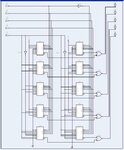
As you can see, not pretty. You can see why the chip was in fact a ROM. To see how complicated things can get, here is an image of the schematic necessary for just one of the output pins, in this case Y2:

You would need to create something similar for each pin, although Y5 wouldn't be too hard.
Anyway, an interesting exercise and one I hope will be of some value to those learning logic circuits.
Cheers, Mark
It dawned on me that writing out the logic statements for these 5 inputs wouldn't be that hard, and that creating the actual logic circuit for each output also wouldn't be that hard. So, for those interested, here are the logic statements. My inputs are the actual binary numbers, not the pin inputs to the chip. So if DCBA = 0110, that'd be binary 6. I'll call my outputs Y0 thru Y6, but since Y0 = A (the LSB's in binary and BCD are always the same), that makes Y1 the second BCD number, but also the correctly named first output of the chip. Also, A is A, A' is NOT A.
Y0 = A
Y1 = F'ED'C'B' + F'E'DCB' + F'EDC'B + FEDC'B' + F'E'D'B + FE'D'B' + F'D'CB + FD'CB' + FE'DB + FDCB
Y2 = FE'D'C'B + FED'CB + E'D'CB' + F'EC'B' + F'E'CB + F'EDC' + EDC'B' + FE'DC
Y3 = F'E'DC'B' + F'ED'C'B + FED'C'B' + F'EDCB' + FE'D'CB + FEDC'B
Y4 = F'ED'C' + F'E'DB + F'E'DC + F'DCB + FEDC' + FE'D' + FD'B + FD'C
Y5 = FE'D' + F'EC +F'ED + EDC
As you can see, not pretty. You can see why the chip was in fact a ROM. To see how complicated things can get, here is an image of the schematic necessary for just one of the output pins, in this case Y2:
You would need to create something similar for each pin, although Y5 wouldn't be too hard.
Anyway, an interesting exercise and one I hope will be of some value to those learning logic circuits.
Cheers, Mark
Last edited by a moderator: