wjxcom
Full Member level 5
Hi all: I am designing a full differential amplifier, the DC GAIN is 45dB, and the GBW is 403MHz, PHASE MARGIN is 66°
During the transient analysis, I use the following statement as the input of the OPA:
VID VID 0 PWL (0 0V 4U 0V 4.0000001U 1V 8U 1V 8.0000001U 0V TD=0)
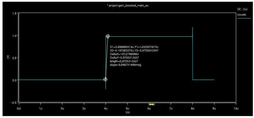
but when I observe the output wave, the maximum value of the output port is only 0.97V, other than o.9999V.
At the save time, the settle time is too long. It's cost 108ns to get the maximux value, i.e. 0.97V.
How can I improve the maximum value and the settle time of the OPA?
Help me please, thanx!!
The netlist of the OPA is the following:
* Project GAIN_BOOSTED_MAIN_TR
* Mentor Graphics Wirelist Created with Version 6.3.17
* Inifile :
* Options : -j -.sp -z -h -n -d -w -m -x -p -k -s
* Levels :
*
* Definition for project BALUN
.SUBCKT BALUN C D N P
V1 P NEV1 DC=0
F2 D 0 CCCS V2 -0.5
E1 NEV1 C VCVS D 0 0.5
E2 NEV2 N VCVS D 0 0.5
V2 C NEV2 DC=0
F1 D 0 CCCS V1 -0.5
* CROSS-REFERENCE 1
* GND = 0
.ENDS
* Definition for project BIAS_2STAGE
.SUBCKT BIAS_2STAGE AVDD AVSS IB VBND VBNU VBPD VBPU
MNB7 N1N344 N1N344 AVSS AVSS NM L=2U W=2.1U
MNB6 N1N487 N1N487 N1N344 AVSS NM L=4U W=2.1U
MNB4 VP N1N344 AVSS AVSS NM L=2U W=2.1U
MPB5 VP VP VBPU AVDD PM L=2U W=6.5U
MPB1 N1N342 VBPD AVDD AVDD PM L=2U W=6.5U
MPB3 VBPD VBPU N1N342 AVDD PM L=0.5U W=6.5U
MPB2 VBPU VP VBPD AVDD PM L=4U W=6.5U M=1
MPB4 VN VBPD AVDD AVDD PM L=2U W=6.5U
MNB1 VN VN VBNU AVSS NM L=2U W=2.1U M=1
MNB2 VBNU VN VBND AVSS NM L=8U W=2.1U M=1
MNB3 VBND VBNU N1N343 AVSS NM L=0.5U W=2.1U M=1
MNB5 N1N343 VBND AVSS AVSS NM L=2U W=2.1U M=1
MP1 N1N456 N1N456 AVDD AVDD PM L=2U W=6.5U
MP2 IB IB N1N456 AVDD PM L=2U W=6.5U
MP3 N1N487 N1N456 AVDD AVDD PM L=2U W=6.5U
* CROSS-REFERENCE 1
* GND = 0
.ENDS
* Definition for project INV
.SUBCKT INV A S V Y
MP Y A V V PM L=0.5U W=3U M=1
MN Y A S S NM L=0.5U W=1.5U M=1
* CROSS-REFERENCE 1
* GND = 0
.ENDS
* Definition for project GAIN_BOOSTED_MAIN
.SUBCKT GAIN_BOOSTED_MAIN AVDD AVSS OUTN OUTP VBND VBNU VBPD VBPU VCMFB VIN VIP
M1 VIPN VIN N1N514 N1N514 PM L=0.5U W=6.5U M=30
M2 VIPP VIP N1N514 N1N514 PM L=0.5U W=6.5U M=30
M9 VIPN VCMFB AVSS AVSS NM L=2U W=2.1U M=100
M10 VIPP VCMFB AVSS AVSS NM L=2U W=2.1U M=100
M7 OUTP VBNU VIPN AVSS NM L=0.5U W=2.1U M=30
M8 OUTN VBNU VIPP AVSS NM L=0.5U W=2.1U M=30
M3 VINP VBPD AVDD AVDD PM L=2U W=6.5U M=50
M4 VINN VBPD AVDD AVDD PM L=2U W=6.5U M=50
M5 OUTP VBPU VINP VINP PM L=0.5U W=6.5U M=20
M6 OUTN VBPU VINN VINN PM L=0.5U W=6.5U M=20
M0 N1N514 VBPD AVDD AVDD PM L=2U W=6.5U M=100
* CROSS-REFERENCE 1
* GND = 0
.ENDS
* Definition for project CMFB-VB_IDEAL
.SUBCKT CMFB-VB_IDEAL AVDD AVSS CK1 CK2 VBO VCM VCMFB VON VOP
RON VON N1N8 1G
E1 VCMFB VBO VCVS N1N8 VCM 1
ROP VOP N1N8 1G
* CROSS-REFERENCE 1
* GND = 0
.ENDS
XBALUN2 OUTC OUTD VON VOP BALUN
XBALUN1 VIC VID VN VP BALUN
CL1 VON AVSS 1.5P
CL2 VOP AVSS 1.5P
C4 VIN VOP 1P
C3 VIP VON 1P
C2 VN VIN 1P
C1 VP VIP 1P
V1I162 AVSS 0 DC=0V
VID VID 0 PWL (0 0V 4U 0V 4.0000001U 1V 8U 1V 8.0000001U 0V TD=0)
XBIAS AVDD AVSS IB VBND VBNU VBPD VBPU BIAS_2STAGE
VCK1 CK 0 PULSE (5V 0V 0 10N 10N 0.01U 0.02U)
XINV1 CK AVSS AVDD CLK1 INV
XINV2 CLK1 AVSS AVDD CLK2 INV
X1I260 AVDD AVSS VON VOP VBND VBNU VBPD VBPU VCMFB VIN VIP GAIN_BOOSTED_MAIN
XCMFB AVDD AVSS CLK1 CLK2 VBND VCM VCMFB VON VOP CMFB-VB_IDEAL
V1I274 VCM 0 DC=2.5
IB IB 0 DC=20U
V1I37 AVDD 0 DC=5V
V1I97 VIC 0 DC=2.5V
*.OPTIONS METHD=GEAR CSDF=2 PROBE
.OP TIME=18U
.PROBE TRAN V(OUTC) V(OUTD) V(VIP) V(VIC) V(VN) V(VP)
.TRAN 0.1NS 9U START=0U
.PROTECT
.LIB 'D:\EXERCISE\DESIGNOPA\CSMC05\MODELS\H05MIXDDST02V12.LIB' TT
* DICTIONARY 1
* GND = 0
.END
the output wave is like this:

During the transient analysis, I use the following statement as the input of the OPA:
VID VID 0 PWL (0 0V 4U 0V 4.0000001U 1V 8U 1V 8.0000001U 0V TD=0)
but when I observe the output wave, the maximum value of the output port is only 0.97V, other than o.9999V.
At the save time, the settle time is too long. It's cost 108ns to get the maximux value, i.e. 0.97V.
How can I improve the maximum value and the settle time of the OPA?
Help me please, thanx!!
The netlist of the OPA is the following:
* Project GAIN_BOOSTED_MAIN_TR
* Mentor Graphics Wirelist Created with Version 6.3.17
* Inifile :
* Options : -j -.sp -z -h -n -d -w -m -x -p -k -s
* Levels :
*
* Definition for project BALUN
.SUBCKT BALUN C D N P
V1 P NEV1 DC=0
F2 D 0 CCCS V2 -0.5
E1 NEV1 C VCVS D 0 0.5
E2 NEV2 N VCVS D 0 0.5
V2 C NEV2 DC=0
F1 D 0 CCCS V1 -0.5
* CROSS-REFERENCE 1
* GND = 0
.ENDS
* Definition for project BIAS_2STAGE
.SUBCKT BIAS_2STAGE AVDD AVSS IB VBND VBNU VBPD VBPU
MNB7 N1N344 N1N344 AVSS AVSS NM L=2U W=2.1U
MNB6 N1N487 N1N487 N1N344 AVSS NM L=4U W=2.1U
MNB4 VP N1N344 AVSS AVSS NM L=2U W=2.1U
MPB5 VP VP VBPU AVDD PM L=2U W=6.5U
MPB1 N1N342 VBPD AVDD AVDD PM L=2U W=6.5U
MPB3 VBPD VBPU N1N342 AVDD PM L=0.5U W=6.5U
MPB2 VBPU VP VBPD AVDD PM L=4U W=6.5U M=1
MPB4 VN VBPD AVDD AVDD PM L=2U W=6.5U
MNB1 VN VN VBNU AVSS NM L=2U W=2.1U M=1
MNB2 VBNU VN VBND AVSS NM L=8U W=2.1U M=1
MNB3 VBND VBNU N1N343 AVSS NM L=0.5U W=2.1U M=1
MNB5 N1N343 VBND AVSS AVSS NM L=2U W=2.1U M=1
MP1 N1N456 N1N456 AVDD AVDD PM L=2U W=6.5U
MP2 IB IB N1N456 AVDD PM L=2U W=6.5U
MP3 N1N487 N1N456 AVDD AVDD PM L=2U W=6.5U
* CROSS-REFERENCE 1
* GND = 0
.ENDS
* Definition for project INV
.SUBCKT INV A S V Y
MP Y A V V PM L=0.5U W=3U M=1
MN Y A S S NM L=0.5U W=1.5U M=1
* CROSS-REFERENCE 1
* GND = 0
.ENDS
* Definition for project GAIN_BOOSTED_MAIN
.SUBCKT GAIN_BOOSTED_MAIN AVDD AVSS OUTN OUTP VBND VBNU VBPD VBPU VCMFB VIN VIP
M1 VIPN VIN N1N514 N1N514 PM L=0.5U W=6.5U M=30
M2 VIPP VIP N1N514 N1N514 PM L=0.5U W=6.5U M=30
M9 VIPN VCMFB AVSS AVSS NM L=2U W=2.1U M=100
M10 VIPP VCMFB AVSS AVSS NM L=2U W=2.1U M=100
M7 OUTP VBNU VIPN AVSS NM L=0.5U W=2.1U M=30
M8 OUTN VBNU VIPP AVSS NM L=0.5U W=2.1U M=30
M3 VINP VBPD AVDD AVDD PM L=2U W=6.5U M=50
M4 VINN VBPD AVDD AVDD PM L=2U W=6.5U M=50
M5 OUTP VBPU VINP VINP PM L=0.5U W=6.5U M=20
M6 OUTN VBPU VINN VINN PM L=0.5U W=6.5U M=20
M0 N1N514 VBPD AVDD AVDD PM L=2U W=6.5U M=100
* CROSS-REFERENCE 1
* GND = 0
.ENDS
* Definition for project CMFB-VB_IDEAL
.SUBCKT CMFB-VB_IDEAL AVDD AVSS CK1 CK2 VBO VCM VCMFB VON VOP
RON VON N1N8 1G
E1 VCMFB VBO VCVS N1N8 VCM 1
ROP VOP N1N8 1G
* CROSS-REFERENCE 1
* GND = 0
.ENDS
XBALUN2 OUTC OUTD VON VOP BALUN
XBALUN1 VIC VID VN VP BALUN
CL1 VON AVSS 1.5P
CL2 VOP AVSS 1.5P
C4 VIN VOP 1P
C3 VIP VON 1P
C2 VN VIN 1P
C1 VP VIP 1P
V1I162 AVSS 0 DC=0V
VID VID 0 PWL (0 0V 4U 0V 4.0000001U 1V 8U 1V 8.0000001U 0V TD=0)
XBIAS AVDD AVSS IB VBND VBNU VBPD VBPU BIAS_2STAGE
VCK1 CK 0 PULSE (5V 0V 0 10N 10N 0.01U 0.02U)
XINV1 CK AVSS AVDD CLK1 INV
XINV2 CLK1 AVSS AVDD CLK2 INV
X1I260 AVDD AVSS VON VOP VBND VBNU VBPD VBPU VCMFB VIN VIP GAIN_BOOSTED_MAIN
XCMFB AVDD AVSS CLK1 CLK2 VBND VCM VCMFB VON VOP CMFB-VB_IDEAL
V1I274 VCM 0 DC=2.5
IB IB 0 DC=20U
V1I37 AVDD 0 DC=5V
V1I97 VIC 0 DC=2.5V
*.OPTIONS METHD=GEAR CSDF=2 PROBE
.OP TIME=18U
.PROBE TRAN V(OUTC) V(OUTD) V(VIP) V(VIC) V(VN) V(VP)
.TRAN 0.1NS 9U START=0U
.PROTECT
.LIB 'D:\EXERCISE\DESIGNOPA\CSMC05\MODELS\H05MIXDDST02V12.LIB' TT
* DICTIONARY 1
* GND = 0
.END
the output wave is like this: