Continue to Site

Welcome to EDAboard.com

Welcome to our site! EDAboard.com is an international Electronics Discussion Forum focused on EDA software, circuits, schematics, books, theory, papers, asic, pld, 8051, DSP, Network, RF, Analog Design, PCB, Service Manuals... and a whole lot more! To participate you need to register. Registration is free. Click here to register now.

A low cost lockin amplifier using off the shelf components: PCB layout audit

Status
Not open for further replies.

randomshinichi

Newbie level 6
Newbie level 6
Joined
Jul 23, 2013
Messages
13
Helped
0
Reputation
0
Reaction score
0
Trophy points
1
Visit site
Activity points
164


Disclaimer: this is for my bachelor's thesis, so before anyone posts, yes, I'm probably out of my depth.

A lockin amplifier can pick out a signal from noise that's orders of magnitude larger than it. But in order to do that, it needs a reference signal that is the same frequency and phase as the signal to pick out. Generally what's done is that the reference signal is also generated by the lockin amplifier, used to drive some system, and the system's response goes into the lockin amplifier, which then does some fancy math to pick out the signal.

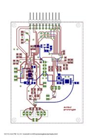
After many nights and cursing, I managed to come up with a PCB using a few components from MAXIM (for simplicity's sake). The instrumentation amplifier picks up the signal, amplifies it, gives it to the ADC, which will digitize it and transfer over SPI to an Arduino Due, which will do the heavy processing. The Arduino Due at the same time outputs a reference signal which the DAC will output, with an opamp to help it along.

As you can see, the intended purpose of this board means that it'll have to be very low-noise, low-distortion... plus I would very much like the first board that I get to work. I think the board has no problems, but other heads might think otherwise. So it would be cool if you guys could have a look over it, see if there are any unintended antennas, if the ground currents will have trouble getting back to GND, that sort of thing (but again, I'm pretty sure I covered anything obvious).

And if anybody knows how to avoid having to drill two vias for the voltage regulators on the other side of the board just to get those pins connected to GND, I would be much obliged. I think they're dirty hacks.

ADC: MAX11040K (24bit)
DAC: MAX5318 (18bit)
Instrumentation Amplifier: MAX4208
Op Amplifier: MAX44246
Supporting parts: MAX1793 5.0V and 3.3V variants, MAX1735 to provide negative voltage, 4 cell LiPo battery (for stable voltage, don't trust the Arduino's supply)

Design notes:
I tried to keep the top part of the PCB strictly digital, and the bottom part analog.

The pins on the top are digital control pins that change settings on the chips. Some are status pins.

The SPI may have to run up to 20MHz, 50MHz in short bursts when communicating with the DAC. length-freq-ri says the SPI lines should be able to run at up to 6GHz, just considering length. But I'm sure there's more to it.

A split ground plane was troublesome (and some articles in Analog Dialogue said it wasn't necessary as long as you make sure the return currents from digital don't cross over into the digital part of the ground plane) so I made one large ground plane.

Power regulation is on the bottom side of the PCB. The 5 pins in the middle are as follows: -3.7V, 0V (GND), 3.7V, 7.4V, 11.1V cells of a LiPo battery

Only channel 1 of the ADC is useful. The rest are there for... well, just for fun and not to waste the 4 channels.

Allowance for a potentiometer on the opamp is there to turn up the gain.

Thanks in advance!
 

Attachments

  • auteur audit.zip
    74.6 KB · Views: 136


Disclaimer: this is for my bachelor's thesis, so before anyone posts, yes, I'm probably out of my depth.

A lockin amplifier can pick out a signal from noise that's orders of magnitude larger than it. But in order to do that, it needs a reference signal that is the same frequency and phase as the signal to pick out. Generally what's done is that the reference signal is also generated by the lockin amplifier, used to drive some system, and the system's response goes into the lockin amplifier, which then does some fancy math to pick out the signal.

After many nights and cursing, I managed to come up with a PCB using a few components from MAXIM (for simplicity's sake). The instrumentation amplifier picks up the signal, amplifies it, gives it to the ADC, which will digitize it and transfer over SPI to an Arduino Due, which will do the heavy processing. The Arduino Due at the same time outputs a reference signal which the DAC will output, with an opamp to help it along.

As you can see, the intended purpose of this board means that it'll have to be very low-noise, low-distortion... plus I would very much like the first board that I get to work. I think the board has no problems, but other heads might think otherwise. So it would be cool if you guys could have a look over it, see if there are any unintended antennas, if the ground currents will have trouble getting back to GND, that sort of thing (but again, I'm pretty sure I covered anything obvious).

And if anybody knows how to avoid having to drill two vias for the voltage regulators on the other side of the board just to get those pins connected to GND, I would be much obliged. I think they're dirty hacks.

ADC: MAX11040K (24bit)
DAC: MAX5318 (18bit)
Instrumentation Amplifier: MAX4208
Op Amplifier: MAX44246
Supporting parts: MAX1793 5.0V and 3.3V variants, MAX1735 to provide negative voltage, 4 cell LiPo battery (for stable voltage, don't trust the Arduino's supply)

Design notes:
I tried to keep the top part of the PCB strictly digital, and the bottom part analog.

The pins on the top are digital control pins that change settings on the chips. Some are status pins.

The SPI may have to run up to 20MHz, 50MHz in short bursts when communicating with the DAC. length-freq-ri says the SPI lines should be able to run at up to 6GHz, just considering length. But I'm sure there's more to it.

A split ground plane was troublesome (and some articles in Analog Dialogue said it wasn't necessary as long as you make sure the return currents from digital don't cross over into the digital part of the ground plane) so I made one large ground plane.

Power regulation is on the bottom side of the PCB. The 5 pins in the middle are as follows: -3.7V, 0V (GND), 3.7V, 7.4V, 11.1V cells of a LiPo battery

Only channel 1 of the ADC is useful. The rest are there for... well, just for fun and not to waste the 4 channels.

Allowance for a potentiometer on the opamp is there to turn up the gain.

Thanks in advance!

Your design is impressive and will possibly work.
I have designed several lock-in amplifiers, better synchonous detectors for Dicke radiometers, to process modulated noise and separate it from receiver thermal noise. The principle was described in 1932 by Kolmogorov and used by Dicke in 1946. It is quite simple, an analog multiplier multiplies sample (reference) pulses by those under noise, then integrates it. Resulting slow DC output is proportional to signal amplitude and REQUIRES adjusting the phase between the multiplied signals (pulses) to work properly.

If you circuit does just this, it will work. I am no expert in digital processing. I think it must first operate well in analog, then you can digitize whatever you want at any step. THe best way to test your design is - make a signal source, put a good attenuator to it, and try how deep in noise it can be retrieved.
 

Status
Not open for further replies.

Similar threads

Part and Inventory Search

Welcome to EDABoard.com

Sponsor

Back
Top