konrad_gom
Junior Member level 1

- Joined
- Dec 15, 2010
- Messages
- 17
- Helped
- 0
- Reputation
- 0
- Reaction score
- 0
- Trophy points
- 1,281
- Activity points
- 1,422
Hello,
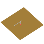
I design 868MHz IFA antenna. It should be placed in one corner of 160x160mm PCB. Small part of GND under the antenna structure is destinated for antenna GND. On the rest part of PCB will be elements and also GND. So can I set whole surface of PCB as a metal (copper)? Are the simulations done OK? What did I wrong?
I attach my design and results.
View attachment 868MHz.rar

