Continue to Site

Welcome to EDAboard.com

Welcome to our site! EDAboard.com is an international Electronics Discussion Forum focused on EDA software, circuits, schematics, books, theory, papers, asic, pld, 8051, DSP, Network, RF, Analog Design, PCB, Service Manuals... and a whole lot more! To participate you need to register. Registration is free. Click here to register now.

4 Phases Non-Overlapping Clock Generator

Status
Not open for further replies.

a7m3d

Newbie level 3
Joined
Dec 12, 2010
Messages
4
Helped
0
Reputation
0
Reaction score
0
Trophy points
1,281
Activity points
1,304
How to implement/design 4 phases non-overlapping clock generator?
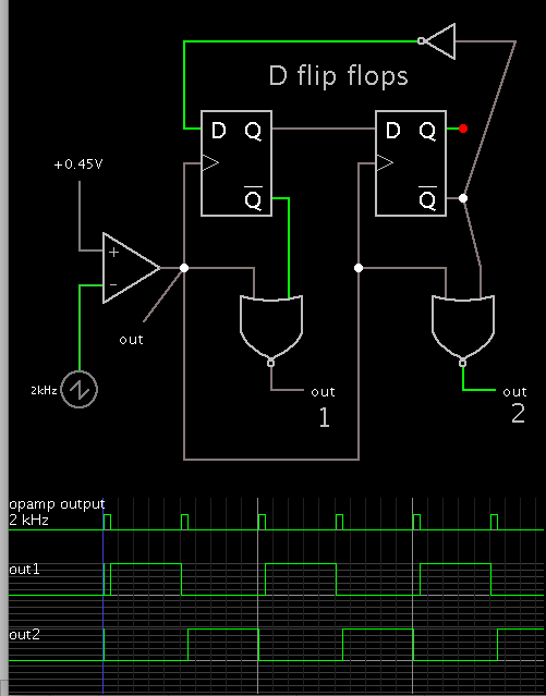
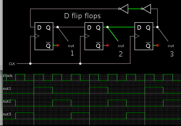
I found this figure without enough details about the implementation. I need a clear reference to build the 4 phases non-overlapping clock generator or in general n phases non-overlapping clock generators for example a 3 phases non-overlapping clock generator.

unnamed.png
 

Your shift register is a start. By adding the right logic gates, a single pulse train is rotated through all outputs.


By adjusting the clock's duty cycle, you change the spacing between the outputs.

This illustrates a concept for 2 outputs. It should be easy to extend it to 4 outputs.
 

The feedback between the 2 flip-flops reserves the state of the output of the 2nd flip-flop. If Q2=0: -> D1=0 -> Q1=0 -> D2=0.
I do not know if I missed something. I will appropriate any help. Thanks.
 

The output of the 4 flip flops is zero, they reserve this state every cycle.
unnamed2.png
 

The problem is not is the NOR gates, the output of the 4 D flip-flops is the same Q1=Q2=Q3=Q4=0. CLK NOR Q(1 or 2 or 3 or 4) will give the same result which is the CLK complement. I do not know if I missed something. Thank you very much.
 

The problem is not is the NOR gates, the output of the 4 D flip-flops is the same Q1=Q2=Q3=Q4=0. CLK NOR Q(1 or 2 or 3 or 4) will give the same result which is the CLK complement. I do not know if I missed something. Thank you very much.

Yes, now I am getting a similar result with my simulation. It does not know what initial state to assign the long wire going the length of the circuit.

I tried a few things, attempting to obtain a sensible output. It worked when I put 2 inverters in a row.


Simulators are prone to these types of errors.
 

You see the ways to make like a Johnson Counter sequence .
Synchronous counter decoder, rotating serial shift register.

Unknown Setup/hold times can produce unpredictable results.

But, if you wanted the edges to be non-overlapping as well as each state, then there must be a dead-band between output phases, such as used in full bridge drivers to prevent shoot-thru.

If that were the case, a monopulse or one-shot on the active clock edge can be used to AND or disable the outputs.
 

Here's an example based on a johnson counter. The frequency of the output will be half the LO frequency.


The duty cycle of the LO (the reference clock) should be 50%. If your clock source is not 50%, then use another flip flop as a frequency divider.
 

Status
Not open for further replies.

Similar threads

Part and Inventory Search

Welcome to EDABoard.com

Sponsor

Back
Top