Benn Ng
Newbie level 6

- Joined
- Mar 25, 2015
- Messages
- 11
- Helped
- 0
- Reputation
- 0
- Reaction score
- 0
- Trophy points
- 1
- Activity points
- 103
hi guys this is my first time using this forum. will appreciate the helps given to me.
i got a project that require me to control a BLDC that is given to me MT2826 from tigermotor
mosfet driver using irs2336d
controller using arduino uno.
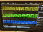
the pwm signal generated out by the arduino uno is attached.
step 1
- the pwm signal from the controller will be fed into a 12.5khz low pass filter that will help to filter out the 32khz sampling frequency.
step 2
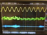
- the output of the filter circuit as attached that is 120deg phase apart is fed into a comparator in this case using LM339N. a voltage divider will be used to compare the dc reference to the input of the comparator. 2 comparator will be used for a single low pass filter that act like a single phase.
Vcc of the voltage divider is 3.3V
r1= 10kohm
r2= 22kohm
r3= 33kohm
[]comparator1 - midpoint of (r1+r2) and r3 will be fed into the -ve terminal of the comparator while the +ve will be the filter signal after the low pass filter.
[]comparator2 - midpoint of r1 and (r2+r3) will be fed into the +ve terminal of the comparator while the -ve will be the filter signal after the low pass filter.
The additional terminal for the comparators will see a reference DC voltage. It will decide the dead timein-between the transitions for the signal routing.
the output of comparator should be a square wave that change frequency with response to the output of the arduino pwm.
step 3
-comparator1 output will be fed into a NAND1 gates 1st input while the 2nd input will be the original PWM directly from the arduino and the final output will be the both input of the NAND2 to to invert back like a AND gate
-comparator2 output will be fed into a NAND3 st input while the 2nd input will be the original PWM directly from the arduino and the final output will be the both input of the NAND4 to to invert back like a AND gate.
NAND gate ic used 74hc00n
This allows the square waveto act as an enable for the signal to pass only when desired. When both the PWM and the enable are high,the logic output will be high. When one is low, the output is low. The resulting signal is a replica of theenable signal, but instead of being consistently high for a given duty cycle, the PWM will be visible during this time.
attached is the waveform. i did not got the square waveform. hope to get some help here. thanks you!


