Continue to Site

Welcome to EDAboard.com

Welcome to our site! EDAboard.com is an international Electronics Discussion Forum focused on EDA software, circuits, schematics, books, theory, papers, asic, pld, 8051, DSP, Network, RF, Analog Design, PCB, Service Manuals... and a whole lot more! To participate you need to register. Registration is free. Click here to register now.

Using SPI Flash with STM32F407VGT6

Status
Not open for further replies.

ogulcan123

Member level 5
Joined
Apr 23, 2011
Messages
81
Helped
0
Reputation
0
Reaction score
0
Trophy points
1,286
Location
Istanbul, Turkey
Activity points
2,024
Hi,

I have Winbond W25Q64FVSSIG, an 8-Mbyte SPI flash, connected to STM32F407VGT6, a 32bit ARM Cortex M4 MCU.

I'm using the MCU as a webserver, so I'm planning to use the SPI flash to store the web page content and some data logs. Therefore, I guess I need to apply a FatFs to whole chip, or some of it if possible.

The problem is I cannot find a way to initialize the MCUs SPI interface to communicate with the SPI Flash chip. There are some documents and examples on the net, but none of them really helped.

Here is how I connected the chip (Although I couldn't test, guess there is no problem with that):
SPI_Flash_SCH.JPG

I'm using STM32F4 standard libraries and the corresponding library file is "stm32f4xx_spi.c" file.
In this file, it explains how to use the driver, but I couldn't apply what is written in the third and fourth items, which are as follow:

-----------------------------------------------------------------------------------------------------------------------
* 3. Peripherals alternate function:
* - Connect the pin to the desired peripherals' Alternate
* Function (AF) using GPIO_PinAFConfig() function
* - Configure the desired pin in alternate function by:
* GPIO_InitStruct->GPIO_Mode = GPIO_Mode_AF
* - Select the type, pull-up/pull-down and output speed via
* GPIO_PuPd, GPIO_OType and GPIO_Speed members
* - Call GPIO_Init() function
* In I2S mode, if an external clock source is used then the I2S CKIN pin
* should be also configured in Alternate function Push-pull pull-up mode.
*
* 4. Program the Polarity, Phase, First Data, Baud Rate Prescaler, Slave
* Management, Peripheral Mode and CRC Polynomial values using the SPI_Init()
* function.
* In I2S mode, program the Mode, Standard, Data Format, MCLK Output, Audio
* frequency and Polarity using I2S_Init() function.
* For I2S mode, make sure that either:
* - I2S PLL is configured using the functions RCC_I2SCLKConfig(RCC_I2S2CLKSource_PLLI2S),
* RCC_PLLI2SCmd(ENABLE) and RCC_GetFlagStatus(RCC_FLAG_PLLI2SRDY).
* or
* - External clock source is configured using the function
* RCC_I2SCLKConfig(RCC_I2S2CLKSource_Ext) and after setting correctly the define constant
* I2S_EXTERNAL_CLOCK_VAL in the stm32f4xx_conf.h file.
-----------------------------------------------------------------------------------------------------------------------

Is there anyone that can help with the proper initialization and use according to the purpose I explained?

Links:
STM32F407xx Datasheet:
http://www.st.com/content/ccc/resou...df/jcr:content/translations/en.DM00037051.pdf

W25Q64FVSSIG Datasheet:
http://www.winbond.com/resource-files/w25q64fv revq 06142016.pdf

stm32f4xx_spi.c library file:
http://github.com/dbridges/stm32f4-discovery-lib/blob/master/StdPeriph/src/stm32f4xx_spi.c


Tags: STM32F4, SPI Flash, SPI Serial Flash, ARM Cortex M4, W25Q64FVSSIG
 

SPI flash uses standard SPI mode 0 or 3, not I2S (a protocol for audio chips). The device is very fast and can probably use any available ARM SPI clock, in case of doubt use moderate clock frequency, e.g. 10 - 20 MHz.

You have 50 ohm SCK parallel termination in your schematic which can hardly be driven by the ARM clock output. If you expect reflections with longer PCB traces, place a series termination (e.g. 50 ohm) near the CPU and no termination at the flash side.
 

Thanks FvM, I will revise the hardware part, I actually took it somewhere and not really sure if correct. Those are 100 ohms pull-up and pull-down resistors. Does it mean 50 ohms although they go different branches?


I dig a little more, and managed to write some initialization without any compiler errors. Now I'm trying to figure out how to use DMA to write into SPI flash.

Here is my initialization part (uncomplete):


Code C - [expand]
1
2
3
4
5
6
7
8
9
10
11
12
13
14
15
16
17
18
19
20
21
22
23
24
25
26
27
28
29
[I] /* Initialize SPI1 for SPI Flash */
     RCC_APB2PeriphClockCmd(RCC_APB2Periph_SPI1, ENABLE);
     SPI_InitTypeDef SPI_InitStruct;
     SPI_InitTypeDef SPI_InitStructure;
     SPI_Init(SPI1, &SPI_InitStruct);
     
     /* Set SPI1 MOSI pin (PB5) as output */
     GPIO_InitTypeDef GPIO_InitStructure;
     GPIO_InitStructure.GPIO_Pin = GPIO_Pin_5;
   GPIO_InitStructure.GPIO_Mode = GPIO_Mode_OUT;
   GPIO_InitStructure.GPIO_OType = GPIO_OType_PP;
   GPIO_InitStructure.GPIO_PuPd = GPIO_PuPd_NOPULL;
   GPIO_InitStructure.GPIO_Speed = GPIO_Speed_100MHz;
   GPIO_Init(GPIOB, &GPIO_InitStructure);
     
     /* Set SPI1 MISO pin (PB4) as input */
     GPIO_InitStructure.GPIO_Pin = GPIO_Pin_4;
   GPIO_InitStructure.GPIO_Mode = GPIO_Mode_IN;
   GPIO_InitStructure.GPIO_OType = GPIO_OType_PP;
   GPIO_InitStructure.GPIO_PuPd = GPIO_PuPd_NOPULL;
   GPIO_InitStructure.GPIO_Speed = GPIO_Speed_100MHz;
   GPIO_Init(GPIOB, &GPIO_InitStructure);
     
     SPI_Cmd(SPI1, ENABLE);
     
     DMA_InitTypeDef DMA_InitStruct;
     DMA_Init(DMA1_Stream0, &DMA_InitStruct);
     
     FLASH_Unlock();[/I]

 
Last edited by a moderator:

I suspect that you need to expand a bit on the SPI configuration. The SPI_InitTypeDef struct contains 11 fields that are used to configure the SPI peripheral.
Of course it is possible that the default settings are exactly what you want (if so I would suggest a comment to that effect in your code) but typically you need to set the clock polarity and phase, data size and the clock rate.
Susan
 
Hi,
Take as a reference this library. I wrote it few years ago, but I remember that it works. Registers definitions you will find in datasheet.
Code:
unsigned char SPI_EEPROM_JEDEC_CHECK (SPI_TypeDef* SPIx)
{
	unsigned char tmp=0;
	PIN_OFF(CS_Pin);
	SPI_SendByte(SPIx, JEDEC_ID_CMD);
	if (SPI_ReadByte(SPIx,0)!=0xBF) tmp++;
	if (SPI_ReadByte(SPIx,0)!=0x25) tmp++;
	if (SPI_ReadByte(SPIx,0)!=0x41) tmp++;
	PIN_ON(CS_Pin);
	if (tmp) return JEDEC_ERROR_MISMATCH; else return SUCCESS;
}
Code:
void SPI_EEPROM_SEND_CMD (SPI_TypeDef* SPIx, unsigned char CMD)
{
	PIN_OFF(CS_Pin);
	SPI_SendByte(SPIx, CMD);
	PIN_ON(CS_Pin);
}
Code:
unsigned char SPI_EEPROM_FULL_ERASE (SPI_TypeDef* SPIx, unsigned long capacity)
{
	SPI_EEPROM_WRITE_REG(SPIx,WRITE_STATUS_CMD, 0);
	SPI_EEPROM_SEND_CMD(SPIx, WRITE_ENABLE_CMD);
	PIN_OFF(CS_Pin);
	SPI_SendByte(SPIx, FULLERASE_CMD);
	delay_ms(CHIP_ERASE_TIME_ms);
	PIN_ON(CS_Pin);
	return SPI_EEPROM_BLANK_CHECK(SPIx);
}
Code:
unsigned long SPI_EEPROM_WRITE_DATA (SPI_TypeDef* SPIx, unsigned long start_adrs, unsigned long page_size)
{
	unsigned long cnt, tmp;
	unsigned int dat;
	
	SPI_EEPROM_SEND_CMD(SPIx, EWSR_CMD);

	SPI_EEPROM_WRITE_REG(SPIx,WRITE_STATUS_CMD, 0);

	SPI_EEPROM_SEND_CMD(SPIx, ENABLE_SO_CMD);	

	SPI_EEPROM_SEND_CMD(SPIx, WRITE_ENABLE_CMD);
	
	PIN_OFF(CS_Pin);
	SPI_SendByte(SPIx, AAI_PROG_CMD);
	SPI_SendByte(SPIx, (0xFF0000&start_adrs)>>16);
	SPI_SendByte(SPIx, (0x00FF00&start_adrs)>>8);
	SPI_SendByte(SPIx, (0x0000FF&start_adrs)>>0);
	for (cnt=0; cnt!=page_size; cnt++)
	{
//	 	SPI_SendByte(SPIx, (0xFF00&flower12[cnt])>>8); 	
//	 	SPI_SendByte(SPIx, (0x00FF&flower12[cnt])>>0);
		PIN_ON(CS_Pin);
		PIN_OFF(CS_Pin);
		while (SPI_ReadByte(SPIx,0)!=0xFF);
		PIN_ON(CS_Pin);
	  PIN_OFF(CS_Pin);
	  SPI_SendByte(SPIx, AAI_PROG_CMD);	
	}
 	PIN_ON(CS_Pin);
	SPI_EEPROM_SEND_CMD(SPIx, WRITE_DISABLE_CMD);
	SPI_EEPROM_SEND_CMD(SPIx, DISABLE_SO_CMD);
	

	tmp=0;
	/*
	PIN_OFF(CS_Pin);
	SPI_SendByte(SPIx, FASTREAD_CMD);
	SPI_SendByte(SPIx, (0xFF0000&start_adrs)>>16);
	SPI_SendByte(SPIx, (0x00FF00&start_adrs)>>8);
	SPI_SendByte(SPIx, (0x0000FF&start_adrs)>>0);
	for (cnt=0; cnt!=page_size; cnt++)
	{
	 	//dat=(SPI_ReadByte(SPIx,0)<<8)|(SPI_ReadByte(SPIx,0)<<0);
	 	dat=(SPI_ReadByte(SPIx,0)<<0)|(SPI_ReadByte(SPIx,0)<<8);
		if (dat!=flower1[cnt]) tmp++;
		//if (SPI_ReadByte(SPIx,0)!=0xFF) tmp++;
	}
	PIN_ON(CS_Pin);
	*/
  return tmp; 
}
Code:
unsigned char SPI_EEPROM_STATUS_READ (SPI_TypeDef* SPIx)
{	
	unsigned char tmp;
	PIN_OFF(CS_Pin);
	SPI_SendByte(SPIx, READ_STATUS_CMD);
	tmp=SPI_ReadByte(SPIx, 0);
	PIN_ON(CS_Pin);
	return tmp;
}
Code:
void SPI_EEPROM_WRITE_REG (SPI_TypeDef* SPIx, unsigned char REG, unsigned char DAT)
{
  PIN_OFF(CS_Pin);
	SPI_SendByte(SPIx, REG);
	SPI_SendByte(SPIx, DAT);
	PIN_ON(CS_Pin);
}
Code:
unsigned long SPI_EEPROM_BLANK_CHECK (SPI_TypeDef* SPIx)
{
	unsigned long cnt, tmp;
	tmp=0;
	PIN_OFF(CS_Pin);
	SPI_SendByte(SPIx, FASTREAD_CMD);
	SPI_SendByte(SPIx, 0);
	SPI_SendByte(SPIx, 0);
	SPI_SendByte(SPIx, 0);
	for (cnt=0; cnt!=LASTADDRESS; cnt++) if (SPI_ReadByte(SPIx,0)!=0xFF) tmp++;
	PIN_ON(CS_Pin);
	if (tmp<10) tmp=0;
	return tmp;
}
Code:
void SPI_EEPROM_WRITE_BYTEPAGE (SPI_TypeDef* SPIx, unsigned long start_adrs, unsigned long page_size, unsigned char * data)
{
	unsigned long cnt;
	SPI_EEPROM_SEND_CMD(SPIx, EWSR_CMD);

	SPI_EEPROM_WRITE_REG(SPIx,WRITE_STATUS_CMD, 0);

	SPI_EEPROM_SEND_CMD(SPIx, ENABLE_SO_CMD);	

	SPI_EEPROM_SEND_CMD(SPIx, WRITE_ENABLE_CMD);
	
	PIN_OFF(CS_Pin);
	SPI_SendByte(SPIx, AAI_PROG_CMD);
	SPI_SendByte(SPIx, (0xFF0000&start_adrs)>>16);
	SPI_SendByte(SPIx, (0x00FF00&start_adrs)>>8);
	SPI_SendByte(SPIx, (0x0000FF&start_adrs)>>0);
	for (cnt=0; cnt!=(page_size>>1); cnt++)
	{
	 	SPI_SendByte(SPIx, *data++); 	
	 	SPI_SendByte(SPIx, *data++); 	
		PIN_ON(CS_Pin);
		PIN_OFF(CS_Pin);
		while (SPI_ReadByte(SPIx,0)!=0xFF);
		PIN_ON(CS_Pin);
	  PIN_OFF(CS_Pin);
	  SPI_SendByte(SPIx, AAI_PROG_CMD);	
	}
 	PIN_ON(CS_Pin);
	SPI_EEPROM_SEND_CMD(SPIx, WRITE_DISABLE_CMD);
	SPI_EEPROM_SEND_CMD(SPIx, DISABLE_SO_CMD);
}
Code:
void SPI_EEPROM_READ_STRING (SPI_TypeDef* SPIx, unsigned long start_adrs,
	unsigned char * data, unsigned long String_Len)
{
	unsigned long cnt;
	PIN_OFF(CS_Pin);
	SPI_SendByte(SPIx, FASTREAD_CMD);
	SPI_SendByte(SPIx, (0xFF0000&start_adrs)>>16);
	SPI_SendByte(SPIx, (0x00FF00&start_adrs)>>8);
	SPI_SendByte(SPIx, (0x0000FF&start_adrs)>>0);
	for (cnt=0;cnt!=String_Len;cnt++) *data++=SPI_ReadByte(SPIx,0);
	PIN_ON(CS_Pin);
}
 

Also, picking up on your comment in the first post that you need to use a 'FatFS' for the chip, I don't agree with this.
Using a FatFS has the advantage that you defer the placement of the actual data to the FatFS library layer and just reference everything as though it were a file. However, as people with SD cards can testify, this requires updating the tables in a known location of the chip for every write access and this has the potential of using up the minimum 100,000 erase/write counts in that part of the memory. Also you will meed more than a simplistic FatFS implementation to spread the usage around the rest of the memory.
On the other hand, if you are not going to erase a 'web page' once you have saved it, then you can device a simple direct access scheme yourself.
Data logs might be a bit of an issue except if they are 'write once' in which case you can use a simple scheme to locate the end of the current log and then simply add to the end of it. When the area allocated to the log is filled, you can then erase the whole lot and start again. Depending on the size of the log entries, the number of updates and the space you allocate to the log, this can spread the 'write' load of the memory over a large area and therefore extend the life of the device.
Another idea: if the memory you are using only has (a minimum) 100,000 erase/write cycles, then why not use a removable device such as an SD card or USB drive. That way you can use some other computer every now and then to duplicate the information onto a new one and effectively 'reset' the erase/write count for the cells/device while retaining the information and also providing a backup. Such a scheme would require a FatFS (or similar) storage scheme to allow it to be read (easily) by a computer but you were considering that option anyway.
Susan
 

Thanks for the replies.

I followed the SPI_InitTypeDef struct fields as you suggested Susan and it worked after some trials.

You might be right about the file system, however HTML files are just files and I need a file system to put them there as far as I know. Is there any other way?


If the memory you are using only has (a minimum) 100,000 erase/write cycles, then why not use a removable device such as an SD card or USB drive.
I'm actually using micro SD card for data logs so that in an emergency situation, the logs can be read plugging into a PC.


Now, I can read and write bytewise anything but the problem is I'm using SPI1 which is controlled by APB2 and it has 21MB of address dedicated. It seem it doesn't have a relationship with AHB3 clock which has a broader address dedicated (more than 1GB).

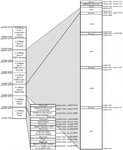
Here is the memory map:
stm32f407 memory map.jpg

So do I need to use another kind of memory anternative which I can connect to FSMC, or is it possible to somehow direct the addresses to SPI1 port from the AHB3 part?
 

Here are my current initialization and trial codes:

Code:
	 /* Initialize SPI1 for SPI Flash */
	 RCC_APB2PeriphClockCmd(RCC_APB2Periph_SPI1, ENABLE);		// SPI1 is located in APB2 bus
	 SPI_InitStruct.SPI_Direction = SPI_Direction_2Lines_FullDuplex;
	 SPI_InitStruct.SPI_Mode = SPI_Mode_Master;					// The device is master
	 SPI_InitStruct.SPI_DataSize = SPI_DataSize_8b; 				// The Winbond W25Q64FVSSIG is 8 bits
	 SPI_InitStruct.SPI_CPOL = SPI_CPOL_Low;					// SPI_CPOL_Low OR SPI_CPOL_High
	 SPI_InitStruct.SPI_CPHA = SPI_CPHA_1Edge;					// Choose clock phase: SPI_CPHA_1Edge OR SPI_CPHA_2Edge
	 SPI_InitStruct.SPI_NSS = SPI_NSS_Soft;					// Slave select: SPI_NSS_Soft OR SPI_NSS_Hard
	 SPI_InitStruct.SPI_BaudRatePrescaler = SPI_BaudRatePrescaler_4;
	 SPI_InitStruct.SPI_FirstBit = SPI_FirstBit_MSB;
	 SPI_InitStruct.SPI_CRCPolynomial = 7;
	 SPI_Init(SPI1, &SPI_InitStruct);
	 
	 /* Set SPI1 MOSI pin (PB5) as output */
	 GPIO_InitStructure.GPIO_Pin = GPIO_Pin_5;
   GPIO_InitStructure.GPIO_Mode = GPIO_Mode_OUT;
   GPIO_InitStructure.GPIO_OType = GPIO_OType_PP;
   GPIO_InitStructure.GPIO_PuPd = GPIO_PuPd_NOPULL;
   GPIO_InitStructure.GPIO_Speed = GPIO_Speed_2MHz;	// SPI speed is 42 Mbit/s, 8 bits data size => Less than 42/8=5.25
   GPIO_Init(GPIOB, &GPIO_InitStructure);
	 
	 /* Set SPI1 MISO pin (PB4) as input */
	 GPIO_InitStructure.GPIO_Pin = GPIO_Pin_4;
   GPIO_InitStructure.GPIO_Mode = GPIO_Mode_IN;
   GPIO_InitStructure.GPIO_OType = GPIO_OType_PP;
   GPIO_InitStructure.GPIO_PuPd = GPIO_PuPd_NOPULL;
   GPIO_InitStructure.GPIO_Speed = GPIO_Speed_2MHz;
   GPIO_Init(GPIOB, &GPIO_InitStructure);
	 
	 SPI_Cmd(SPI1, ENABLE);
	 
	 DMA_Init(DMA1_Stream0, &DMA_InitStruct);


Code:
		 i_spi=0;
		 for(spi_address=0x40013021;spi_address<=0x400133FF;spi_address++)
		 {
			 FLASH_Unlock();
			 status = FLASH_ProgramByte(spi_address, i_spi);
			 FLASH_Lock();
			 SPI_buffer = *(uint8_t*) spi_address;
			 if(SPI_buffer!=0){
				 TRACE_INFO("\r\n**SPI** 0x%08x W:%d R:%d", spi_address, i_spi, SPI_buffer);
				 if (status==8) {
					 TRACE_INFO("  OK");
				 }
				 else {
					 TRACE_INFO("  FAILED!");
				 }
			 }
			 i_spi++;
			 i_spi = i_spi%256;
		 }

I tested the pins of the SPI flash chip, and there is no signal in any of them. The CLK and NSS pins are 3.3V, others are 0V.

What do you think is wrong here? Can it be the hardware connections? I also tried removing the pull-up resistors.
 

I must admit that I've always used the HAL API which also requires the SPI_HandleTypeDef which references the SPI_InitTypeDef (equivalent to your SPI_InitStructure type) but also includes all of the buffer pointers and DMA handles etc..
However I can't see where you have told the pins that they need to carry the alternate function. With the HAL GPIO init structure there is an 'Alternate' field that lets you map the peripheral (or whatever) function to the pin.
Also don't you need to set up the GPIO pins for the MOSI, MISO and SCK functions as a minimum? I can only see you mapping 2 pins - you need to map PB3 as SPI1_SCK as well. You mention NSS - that will need to be mapped also.
Susan
 
Thanks Susan, that really helped.

you need to map PB3 as SPI1_SCK as well. You mention NSS - that will need to be mapped also.

Should I map these pins as I do it in the MOSI pin mapping? Also do you see any mistakes in the mapping of MOSI and MISO?
 

Yes BUT I can't see where you are actually telling the PB4 and PB5 pins that they are to map to the 'alternate' functions of the MISO and MOSI (respectively).
There is probably a field in the GPIO_InitStructure with a name something like GPIO_Alternate and you needs to set that to whatever the appropriate code is. If not then there is probably a function named something like GPIO_PinRemapConfig that will do the job for you.
Also you may need to change the GPIO_Mode field to a value that references one of the alternate function modes such as GPIO_MODE_AF_PP.
(As you might be able to tell, I'm a way from my reference material and its a long time since I did this so my memory is a bit vague. Should put you on the right path though.)
I suggest that you look at some of the numerous tutorials about programming these devices and how to map the peripherals to the pins - they are quite straight forward when you get the hang of them but there are lots of details to consider. (Flexibility comes at a price!)
Susan
 
Last edited:

Status
Not open for further replies.

Similar threads

Part and Inventory Search

Welcome to EDABoard.com

Sponsor

Back
Top