afz23
Full Member level 3
I am designing an amplifier at 12 GHz,using infineon
Cfy25 device.
Vendor supplied s-param were extracted in following
Manner,using FR4 board.
Note: reference plane position at device lead end,
Leads are 1.1mm long

Since I am using another substrate,Alumina,I need
S-param ,at the package end ,as shown below

I simulated the device leads separately and used ADS
De-embbeding boxes as shown below and extract DUT s-param
Experts please look into this and give your valuable suggestions,to solve this issue.
Because I do not know how ADS deals with s-param
De-embedding,whether it transforms to T parameters
And

But this method did not work, the resulting s-param
Were totally changed,not usable as leads should change little phase and magnitude of s-param,not the entire frequency response itself.
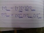
For de-embedding we use following matrix relation
Using transmission parametets
Cfy25 device.
Vendor supplied s-param were extracted in following
Manner,using FR4 board.
Note: reference plane position at device lead end,
Leads are 1.1mm long
Since I am using another substrate,Alumina,I need
S-param ,at the package end ,as shown below
I simulated the device leads separately and used ADS
De-embbeding boxes as shown below and extract DUT s-param
Experts please look into this and give your valuable suggestions,to solve this issue.
Because I do not know how ADS deals with s-param
De-embedding,whether it transforms to T parameters
And
But this method did not work, the resulting s-param
Were totally changed,not usable as leads should change little phase and magnitude of s-param,not the entire frequency response itself.
For de-embedding we use following matrix relation
Using transmission parametets
Attachments
Last edited: