Continue to Site

Welcome to EDAboard.com

Welcome to our site! EDAboard.com is an international Electronics Discussion Forum focused on EDA software, circuits, schematics, books, theory, papers, asic, pld, 8051, DSP, Network, RF, Analog Design, PCB, Service Manuals... and a whole lot more! To participate you need to register. Registration is free. Click here to register now.

[SOLVED] Can anyone help with this H bridge circuit on pspice?

Status
Not open for further replies.

zqbeijing

Newbie level 5
Joined
Jun 7, 2012
Messages
8
Helped
0
Reputation
0
Reaction score
0
Trophy points
1,281
Activity points
1,364
Hello! I'm a newbie on this forum.

I'm currently desinging a h bridge circuit based on a larger scale energy harvester project. Unfortunately, I'm now stucking on the schematic design by using pspice simulation.

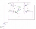
The circuit is actually a quite simple h bridge by using ideal switches as the picture shown in the attachment.

G1 is the voltage controled current source with a sin wave V1 connected to it and drives a voltage difference Vc1 at the output end.

Ideal switches S1-S4 are being used to switch this configuration. The on/off voltages are controled by a sin wave V2 with amplitude equals to 10V and same frequency as the input source to G1. However, I use a limiter to limit this 10V sin wave to +/- 0.4V and make it act as a square wave so the switches can employ.

Therefore, the basic idea of operation should be as following:
1) When V1 reach to a positive peak, V2 also reach to positive peak because they are in same frequency.
2) The square wave reaches to +0.4V simultaneously (no delay at limiter) and this voltage feed in to S1 and S4.
3) S1 and S4 switch on and output of G1 will conduct left to right and the voltage difference Vc1 should be in phase with input V1 because all these should happen at the same time.
4) S1 and S4 switch off and S2/3 switch on, circuit operates in a similar way with another direction.

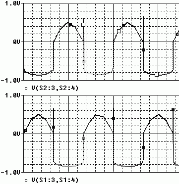
However, the simulation result (also shown in the attachment) is not what I've expected, the waveform of Vc1 has 180 phase shift with V1. I also measured the output voltage from s1 and s2 and they are in different phase as well so I'm sure they won't switch on/off at the same time.

So can any one point out the problem with this design please? I know this might sound retarded, but please help.

Thanks a lot!
 

Attachments

  • bbs_schematic.jpg
    bbs_schematic.jpg
    178 KB · Views: 231
  • bbs_results.jpg
    bbs_results.jpg
    1 MB · Views: 161

Hi why you didn't use mosfets ? what the .... are those that you used ? why you used sine wave and then .... ? it is pretty simple use four vpulse simply !
Best Wishes
Goldsmith
 

- - - Updated - - -

Hi why you didn't use mosfets ? what the .... are those that you used ? why you used sine wave and then .... ? it is pretty simple use four vpulse simply !
Best Wishes
Goldsmith
Thank you for your comments goldsmith.

I wish that I can use mosfets. The reason that I use ideal switches is because my supervisor forced me to do so... quite strange eh?

I tried different types of sources, include sin wave and V pulse, configured to square wave, triangle wave and sawtooth, but the point is, whatever types of source I use, i got similar results. So should there be other things wrong with design?

cheers.
 

What should be the operation frequency and duty cycle and out put voltage ? . if you tell them to me , i can simulate it and show you the result .
Best Wishes
Goldsmith
 

zqbeijing,


You must provide proper delay in order to avoid simultaneous conduction of switches at same side of H-bridge.

Regarding use of switches instead transistors (BJT, MOSFET,IGBT,etc...), makes sense, once the first task is to perform simulation correctly, and then insert real-world devices.


+++
 

What should be the operation frequency and duty cycle and out put voltage ? . if you tell them to me , i can simulate it and show you the result .
Best Wishes
Goldsmith
There is no designated operation frequency and o/p voltage, duty cycle 0.5. According to my supervisor, this test is simply to make V1 in phase with the output Vc1 while according to his idea of the operation of vccs and h bridge they should be.

Do you think there will be something wrong with the theory behind the design?

Thanks for your help.

- - - Updated - - -

zqbeijing,


You must provide proper delay in order to avoid simultaneous conduction of switches at same side of H-bridge.
Regarding use of switches instead transistors (BJT, MOSFET,IGBT,etc...), makes sense, once the first task is to perform simulation correctly, and then insert real-world devices.


+++

Thanks for your comments andre.

What do you mean by provide delay to avoid simultaneous conduction of switches at the same side of h-bridge? Like to place inverting buffer or something?
 

Hi again
Afternoon i'll send it .
And a notation regarding things that andre said : i think he is referring to the dead time to prevent overlapping . as you know each mosfet has dealy time and GS capacitor effect , thus it is pretty bad if you don't create dead time ! because at a little time VDC will connect to the ground .
Best Wishes
Goldsmith
 

Where's the bus voltage source? The waveforms suggests that the node is floating.
 

Where's the bus voltage source? The waveforms suggests that the node is floating.
Hi FvM:
Supply voltage is 10V as shown on the schematic.
It should be alright to perform a simulation.
Thanks

- - - Updated - - -

Hi again
Afternoon i'll send it .
And a notation regarding things that andre said : i think he is referring to the dead time to prevent overlapping . as you know each mosfet has dealy time and GS capacitor effect , thus it is pretty bad if you don't create dead time ! because at a little time VDC will connect to the ground .
Best Wishes
Goldsmith
So I think that is one reason why my supervisor asked me to use ideal switches first because there are some non ideal characteristics by using fets.
One thing I feel extremely confuse is that will V1 and Vc1 actually be in phase according to power electronics and analogue theory..
I realized that my current knowledge is quite basic, but I did not see anything wrong with it.
Any comments my friend?
 

Hi again
I came back ! see below please :
H bridge.JPG
H bridge 2.JPG
But if you want to build this circuit in practice all things will change !
Best Wishes
Goldsmith
 

Supply voltage is 10V as shown on the schematic.
It should be alright to perform a simulation.
Thanks
I agree, that the "10V" node name suggests a DC supply. It would be easy to show the VDC source in the schematic to clear the doubts.

Anyway. You surely agree, that the S1 and S2 switch voltages should sum to 10 V. Please help may to identify this summation in your waveform, see the below detail. In my understanding the waveforms shows |Vbus| < 1 V.

17_1339428612.gif


But if you want to build this circuit in practice all things will change !
No doubt about. But it should work with ideal switches as well. I'm often using switch models for a functional simulation of complex power electronics circuits, e.g. when focussing on the controller design.
 

I agree, that the "10V" node name suggests a DC supply. It would be easy to show the VDC source in the schematic to clear the doubts.

Anyway. You surely agree, that the S1 and S2 switch voltages should sum to 10 V. Please help may to identify this summation in your waveform, see the below detail. In my understanding the waveforms shows |Vbus| < 1 V.

17_1339428612.gif


No doubt about. But it should work with ideal switches as well. I'm often using switch models for a functional simulation of complex power electronics circuits, e.g. when focussing on the controller design.

Thanks! You are right, that 10V node wont give any supply voltage, but actually I found that I don't need a supply voltage because ideal switches will be controled by +/- 0.4 v.

What I want is the voltage generated from the output of that vccs, and I expect to have it in phase with V1. But my result always shows a 180 phase different, the current at + end of G is in phase with V1 but the voltage across the output isn't. Does the vccs model in pspice library behave like this?

- - - Updated - - -

Hi again
I came back ! see below please :
View attachment 75708
View attachment 75709
But if you want to build this circuit in practice all things will change !
Best Wishes
Goldsmith

Thanks for you help, your design really gave me some hints about how to control the switches. But the problem now becomes about the voltage controled current source G1, Do you think the voltage difference across the output of G1 can be in phase with V1?
 

o you think the voltage difference across the output of G1 can be in phase with V1?
What ? are you referring to the voltage across the gate of M1 ? of course it is in phase with vpulse 1 because those are in parallel together . perhaps you're referring to another thing ?
 

What ? are you referring to the voltage across the gate of M1 ? of course it is in phase with vpulse 1 because those are in parallel together . perhaps you're referring to another thing ?
No, i was referring to the voltage across the output ends of voltage controled current source G1 in my shcmatic...now the problem about how the switches can be controled has been solved, i feel confused with the characteristics of that vccs...
 

The polarity of the current source is indicated by an arrow and is according to usual SPICE rules, current flowing from + to - node. In case of doubt, you can refer to the PSPICE user manual.
 

The polarity of the current source is indicated by an arrow and is according to usual SPICE rules, current flowing from + to - node. In case of doubt, you can refer to the PSPICE user manual.

Thank you my friend, by your enlightment I just found out the reason of the phase problem.

I put the wrong side of the voltage marker on the circuit. Because current flows from left to right within the vcccs but right to left at output therefore the + end of Vc is on right side and - end is on left side...

I feel i was so stupid...hahah...

Anyway, thanks so much
 

Status
Not open for further replies.

Similar threads

Part and Inventory Search

Welcome to EDABoard.com

Sponsor

Back
Top